{"title":"Photoresist Removal by an Aluminum Protective Layer to Improve the Performance of Carbon Nanotube Thin-Film Transistors","authors":"Xiao Li, Wenke Wang, Yuejuan Zhang, Feijiu Wang, Yanchun Wang, Linhai Li, Xiaojun Wei, Weiya Zhou and Huaping Liu*, ","doi":"10.1021/acsanm.4c0584810.1021/acsanm.4c05848","DOIUrl":null,"url":null,"abstract":"<p >Photolithography is a key process in the fabrication of carbon nanotube devices. However, the strong interactions between organic photoresists and single-wall carbon nanotube (SWCNT) films result in residual photoresists on their surfaces after lithography, which increases the interfacial resistance between the SWCNTs and between the SWCNTs and the metallic electrodes. To reduce the contamination of the photoresist in the photolithography process, we introduce an ultrathin aluminum metal protective layer to isolate the photoresist and the SWCNT film in the photolithography process, which is prepared via simple thermal evaporation. The protective layer can be removed by etching with the developer and subsequent acid solution without affecting the patterns, while the SWCNT film maintains a clean surface. The resulting SWCNT thin-film transistors exhibit an order of magnitude greater on-state current and carrier mobility than those without the protective layer because a substantial decrease in the resistance between the SWCNTs and between the SWCNT film and the metallic electrodes. This work provides an important scheme for the fabrication of high-performance carbon-based devices.</p>","PeriodicalId":6,"journal":{"name":"ACS Applied Nano Materials","volume":"8 1","pages":"486–494 486–494"},"PeriodicalIF":5.5000,"publicationDate":"2024-12-29","publicationTypes":"Journal Article","fieldsOfStudy":null,"isOpenAccess":false,"openAccessPdf":"","citationCount":"0","resultStr":null,"platform":"Semanticscholar","paperid":null,"PeriodicalName":"ACS Applied Nano Materials","FirstCategoryId":"88","ListUrlMain":"https://pubs.acs.org/doi/10.1021/acsanm.4c05848","RegionNum":2,"RegionCategory":"材料科学","ArticlePicture":[],"TitleCN":null,"AbstractTextCN":null,"PMCID":null,"EPubDate":"","PubModel":"","JCR":"Q2","JCRName":"MATERIALS SCIENCE, MULTIDISCIPLINARY","Score":null,"Total":0}
引用次数: 0
Abstract
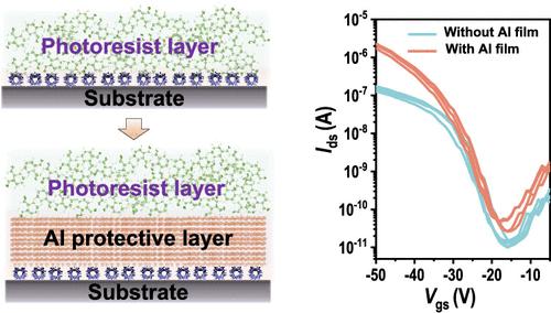
Photolithography is a key process in the fabrication of carbon nanotube devices. However, the strong interactions between organic photoresists and single-wall carbon nanotube (SWCNT) films result in residual photoresists on their surfaces after lithography, which increases the interfacial resistance between the SWCNTs and between the SWCNTs and the metallic electrodes. To reduce the contamination of the photoresist in the photolithography process, we introduce an ultrathin aluminum metal protective layer to isolate the photoresist and the SWCNT film in the photolithography process, which is prepared via simple thermal evaporation. The protective layer can be removed by etching with the developer and subsequent acid solution without affecting the patterns, while the SWCNT film maintains a clean surface. The resulting SWCNT thin-film transistors exhibit an order of magnitude greater on-state current and carrier mobility than those without the protective layer because a substantial decrease in the resistance between the SWCNTs and between the SWCNT film and the metallic electrodes. This work provides an important scheme for the fabrication of high-performance carbon-based devices.
期刊介绍:
ACS Applied Nano Materials is an interdisciplinary journal publishing original research covering all aspects of engineering, chemistry, physics and biology relevant to applications of nanomaterials. The journal is devoted to reports of new and original experimental and theoretical research of an applied nature that integrate knowledge in the areas of materials, engineering, physics, bioscience, and chemistry into important applications of nanomaterials.

 求助内容:
求助内容: 应助结果提醒方式:


