Guozhang Dai*, Yangyang Liu, Yang Xiang, Ziyi Yang, Ying Wang, Yuguang Luo, Tengxiao Xiongsong, Jidong Zhang and Junliang Yang*,
{"title":"van der Waals Epitaxial Growth of Centimeter-Scale CdTe Thin Films for High-Performance Photodetectors","authors":"Guozhang Dai*, Yangyang Liu, Yang Xiang, Ziyi Yang, Ying Wang, Yuguang Luo, Tengxiao Xiongsong, Jidong Zhang and Junliang Yang*, ","doi":"10.1021/acsaelm.4c0175410.1021/acsaelm.4c01754","DOIUrl":null,"url":null,"abstract":"<p >Group II–VI semiconductor CdTe is widely used in optoelectronic devices because of its high absorption coefficient and good chemical stability. High-quality CdTe thin films serve as the foundation for high-performance optoelectronic devices. In this work, centimeter-scale CdTe thin films were synthesized via van der Waals heteroepitaxy on mica substrates using vapor phase transport (VTD), and planar structure photodetectors (PDs) were constructed via depositing the Au electrodes on the surface directly or exfoliated buried interface. The results show that the performance of PDs constructed using a CdTe buried interface is much better than those constructed using a CdTe surface under the light irradiation at the wavelengths of 406, 642, and 808 nm, and the switching ratio can reach up to 2 × 10<sup>4</sup>, with a response of 4.4 A/W and a short response time of 1.5 ms. The smooth interface morphology and a large area of flat and dense surfaces are conducive to carrier transport, showing better performance. Furthermore, flexible PDs are constructed via transferring CdTe thin films onto a poly(ethylene terephthalate) (PET) substrate and exhibit excellent flexibility and stability, which can maintain 96.5% original performance with more than 200 times bending at a curvature radius of 5 mm. The research indicates that the high-quality, centimeter-scale CdTe with buried interface fabricated via van der Waals epitaxial growth is a promising potential candidate in high-performance optoelectronic devices.</p>","PeriodicalId":3,"journal":{"name":"ACS Applied Electronic Materials","volume":"7 1","pages":"277–285 277–285"},"PeriodicalIF":4.7000,"publicationDate":"2024-12-17","publicationTypes":"Journal Article","fieldsOfStudy":null,"isOpenAccess":false,"openAccessPdf":"","citationCount":"0","resultStr":null,"platform":"Semanticscholar","paperid":null,"PeriodicalName":"ACS Applied Electronic Materials","FirstCategoryId":"88","ListUrlMain":"https://pubs.acs.org/doi/10.1021/acsaelm.4c01754","RegionNum":3,"RegionCategory":"材料科学","ArticlePicture":[],"TitleCN":null,"AbstractTextCN":null,"PMCID":null,"EPubDate":"","PubModel":"","JCR":"Q1","JCRName":"ENGINEERING, ELECTRICAL & ELECTRONIC","Score":null,"Total":0}
引用次数: 0
Abstract
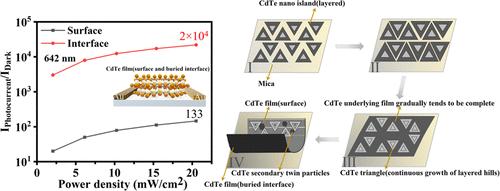
Group II–VI semiconductor CdTe is widely used in optoelectronic devices because of its high absorption coefficient and good chemical stability. High-quality CdTe thin films serve as the foundation for high-performance optoelectronic devices. In this work, centimeter-scale CdTe thin films were synthesized via van der Waals heteroepitaxy on mica substrates using vapor phase transport (VTD), and planar structure photodetectors (PDs) were constructed via depositing the Au electrodes on the surface directly or exfoliated buried interface. The results show that the performance of PDs constructed using a CdTe buried interface is much better than those constructed using a CdTe surface under the light irradiation at the wavelengths of 406, 642, and 808 nm, and the switching ratio can reach up to 2 × 10⁴, with a response of 4.4 A/W and a short response time of 1.5 ms. The smooth interface morphology and a large area of flat and dense surfaces are conducive to carrier transport, showing better performance. Furthermore, flexible PDs are constructed via transferring CdTe thin films onto a poly(ethylene terephthalate) (PET) substrate and exhibit excellent flexibility and stability, which can maintain 96.5% original performance with more than 200 times bending at a curvature radius of 5 mm. The research indicates that the high-quality, centimeter-scale CdTe with buried interface fabricated via van der Waals epitaxial growth is a promising potential candidate in high-performance optoelectronic devices.
期刊介绍:
ACS Applied Electronic Materials is an interdisciplinary journal publishing original research covering all aspects of electronic materials. The journal is devoted to reports of new and original experimental and theoretical research of an applied nature that integrate knowledge in the areas of materials science, engineering, optics, physics, and chemistry into important applications of electronic materials. Sample research topics that span the journal's scope are inorganic, organic, ionic and polymeric materials with properties that include conducting, semiconducting, superconducting, insulating, dielectric, magnetic, optoelectronic, piezoelectric, ferroelectric and thermoelectric.
Indexed/Abstracted:
Web of Science SCIE
Scopus
CAS
INSPEC
Portico

 求助内容:
求助内容: 应助结果提醒方式:


