Solution-processed wafer-scale indium selenide semiconductor thin films with high mobilities
IF 40.9
1区 工程技术
Q1 ENGINEERING, ELECTRICAL & ELECTRONIC
引用次数: 0
Abstract
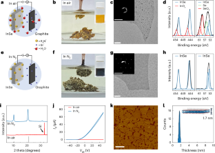
Solution-processed two-dimensional semiconductors could be used to create electronic devices on large scales and at low cost. However, the electronic performance of devices based on such materials is typically below that of devices based on materials grown via high-temperature chemical vapour deposition. Here we report the fabrication of indium selenide (InSe) semiconductor thin films using a colloidal solution of monolayer nanosheets (monolayer purity more than 98%). The InSe thin films are assembled on 4-inch wafers with conformal and intimate van der Waals contacts between the monolayer building blocks. We use the solution-processed films to fabricate InSe transistors that exhibit electron mobilities of 90–120 cm2 V−1 s−1, current on/off ratios of up to 107 and a small current hysteresis. We also show that InSe transistors with oxide encapsulation can remain stable in air for 3 months. Indium selenide semiconductor thin films can be fabricated from a colloidal solution of monolayer nanosheets, and used to create transistors that exhibit electron mobilities of 90–120 cm2 V−1 s−1, current on/off ratios of up to 107 and a small current hysteresis.

溶液处理高迁移率的晶圆级硒化铟半导体薄膜
溶液处理的二维半导体可以用于制造大规模和低成本的电子设备。然而,基于这种材料的器件的电子性能通常低于通过高温化学气相沉积生长的材料的器件。本文报道了利用单层纳米片胶体溶液(单层纯度大于98%)制备硒化铟(InSe)半导体薄膜。InSe薄膜被组装在4英寸的晶圆上,单层构建块之间具有共形和亲密的范德华接触。我们使用溶液处理的薄膜来制造铟硒晶体管,其电子迁移率为90-120 cm2 V−1 s−1,电流开/关比高达107,电流滞后小。我们还表明,采用氧化物封装的InSe晶体管可以在空气中稳定保持3个月。
本文章由计算机程序翻译,如有差异,请以英文原文为准。
求助全文
约1分钟内获得全文
求助全文
来源期刊
Nature Electronics
Engineering-Electrical and Electronic Engineering
CiteScore
47.50
自引率
2.30%
发文量
159
期刊介绍:
Nature Electronics is a comprehensive journal that publishes both fundamental and applied research in the field of electronics. It encompasses a wide range of topics, including the study of new phenomena and devices, the design and construction of electronic circuits, and the practical applications of electronics. In addition, the journal explores the commercial and industrial aspects of electronics research.
The primary focus of Nature Electronics is on the development of technology and its potential impact on society. The journal incorporates the contributions of scientists, engineers, and industry professionals, offering a platform for their research findings. Moreover, Nature Electronics provides insightful commentary, thorough reviews, and analysis of the key issues that shape the field, as well as the technologies that are reshaping society.
Like all journals within the prestigious Nature brand, Nature Electronics upholds the highest standards of quality. It maintains a dedicated team of professional editors and follows a fair and rigorous peer-review process. The journal also ensures impeccable copy-editing and production, enabling swift publication. Additionally, Nature Electronics prides itself on its editorial independence, ensuring unbiased and impartial reporting.
In summary, Nature Electronics is a leading journal that publishes cutting-edge research in electronics. With its multidisciplinary approach and commitment to excellence, the journal serves as a valuable resource for scientists, engineers, and industry professionals seeking to stay at the forefront of advancements in the field.
文献相关原料
公司名称
产品信息
麦克林
In
阿拉丁
Se
阿拉丁
NH4Cl
 求助内容:
求助内容: 应助结果提醒方式:


