Fabrication of Ultra-Low-Loss, Dispersion-Engineered Silicon Nitride Photonic Integrated Circuits via Silicon Hardmask Etching

IF 6.5 1区 物理与天体物理 Q1 MATERIALS SCIENCE, MULTIDISCIPLINARY
Shuai Liu, Yuheng Zhang, Abdulkarim Hariri, Abdur-Raheem Al-Hallak, Zheshen Zhang
{"title":"Fabrication of Ultra-Low-Loss, Dispersion-Engineered Silicon Nitride Photonic Integrated Circuits via Silicon Hardmask Etching","authors":"Shuai Liu, Yuheng Zhang, Abdulkarim Hariri, Abdur-Raheem Al-Hallak, Zheshen Zhang","doi":"10.1021/acsphotonics.4c02172","DOIUrl":null,"url":null,"abstract":"Silicon nitride (Si<sub>3</sub>N<sub>4</sub>) photonic integrated circuits (PICs) have emerged as a versatile platform for a wide range of applications, such as nonlinear optics, narrow-line-width lasers, and quantum photonics. While thin-film Si<sub>3</sub>N<sub>4</sub> processes have been extensively developed, many nonlinear and quantum optics applications require the use of thick Si<sub>3</sub>N<sub>4</sub> films with engineered dispersion, high mode confinement, and low optical loss. However, high tensile stress in thick Si<sub>3</sub>N<sub>4</sub> films often leads to cracking, making the fabrication challenging to meet these requirements. In this work, we present a robust and reliable fabrication method for ultralow-loss, dispersion-engineered Si<sub>3</sub>N<sub>4</sub> PICs using amorphous silicon (a-Si) hardmask etching. This approach enables smooth etching of thick Si<sub>3</sub>N<sub>4</sub> waveguides while ensuring the long-term storage of crack-free Si<sub>3</sub>N<sub>4</sub> wafers. We achieve intrinsic quality factors (<i>Q</i><sub>i</sub>) as high as 25.6 × 10<sup>6</sup>, corresponding to a propagation loss of 1.6 dB/m. The introduction of a-Si hardmask etching along with novel crack-isolation trench designs and fabrication strategies offers notable advantages including high etching selectivity, long-term wafer storage, high yield, and full compatibility with existing well-developed silicon-based semiconductor processes. We demonstrate frequency comb generation in the fabricated microring resonators, showcasing the platform’s potential for applications in optical communication, nonlinear optics, metrology, and spectroscopy. This stable and efficient fabrication method offers high performance with significantly reduced fabrication complexity, representing a remarkable advancement toward mass production of Si<sub>3</sub>N<sub>4</sub> PICs for a wide spectrum of applications.","PeriodicalId":23,"journal":{"name":"ACS Photonics","volume":"67 1","pages":""},"PeriodicalIF":6.5000,"publicationDate":"2025-02-02","publicationTypes":"Journal Article","fieldsOfStudy":null,"isOpenAccess":false,"openAccessPdf":"","citationCount":"0","resultStr":null,"platform":"Semanticscholar","paperid":null,"PeriodicalName":"ACS Photonics","FirstCategoryId":"101","ListUrlMain":"https://doi.org/10.1021/acsphotonics.4c02172","RegionNum":1,"RegionCategory":"物理与天体物理","ArticlePicture":[],"TitleCN":null,"AbstractTextCN":null,"PMCID":null,"EPubDate":"","PubModel":"","JCR":"Q1","JCRName":"MATERIALS SCIENCE, MULTIDISCIPLINARY","Score":null,"Total":0}
引用次数: 0

Abstract

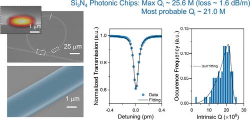
Silicon nitride (Si3N4) photonic integrated circuits (PICs) have emerged as a versatile platform for a wide range of applications, such as nonlinear optics, narrow-line-width lasers, and quantum photonics. While thin-film Si3N4 processes have been extensively developed, many nonlinear and quantum optics applications require the use of thick Si3N4 films with engineered dispersion, high mode confinement, and low optical loss. However, high tensile stress in thick Si3N4 films often leads to cracking, making the fabrication challenging to meet these requirements. In this work, we present a robust and reliable fabrication method for ultralow-loss, dispersion-engineered Si3N4 PICs using amorphous silicon (a-Si) hardmask etching. This approach enables smooth etching of thick Si3N4 waveguides while ensuring the long-term storage of crack-free Si3N4 wafers. We achieve intrinsic quality factors (Qi) as high as 25.6 × 10⁶, corresponding to a propagation loss of 1.6 dB/m. The introduction of a-Si hardmask etching along with novel crack-isolation trench designs and fabrication strategies offers notable advantages including high etching selectivity, long-term wafer storage, high yield, and full compatibility with existing well-developed silicon-based semiconductor processes. We demonstrate frequency comb generation in the fabricated microring resonators, showcasing the platform’s potential for applications in optical communication, nonlinear optics, metrology, and spectroscopy. This stable and efficient fabrication method offers high performance with significantly reduced fabrication complexity, representing a remarkable advancement toward mass production of Si3N4 PICs for a wide spectrum of applications.

Abstract Image

求助全文
约1分钟内获得全文 求助全文
来源期刊
ACS Photonics
ACS Photonics NANOSCIENCE & NANOTECHNOLOGY-MATERIALS SCIENCE, MULTIDISCIPLINARY
CiteScore
11.90
自引率
5.70%
发文量
438
审稿时长
2.3 months
期刊介绍: Published as soon as accepted and summarized in monthly issues, ACS Photonics will publish Research Articles, Letters, Perspectives, and Reviews, to encompass the full scope of published research in this field.
×
引用
GB/T 7714-2015
复制
MLA
复制
APA
复制
导出至
BibTeX EndNote RefMan NoteFirst NoteExpress
×
提示
您的信息不完整,为了账户安全,请先补充。
现在去补充
×
提示
您因"违规操作"
具体请查看互助需知
我知道了
×
提示
确定
请完成安全验证×
copy
已复制链接
快去分享给好友吧!
我知道了
右上角分享
点击右上角分享
0
联系我们:info@booksci.cn Book学术提供免费学术资源搜索服务,方便国内外学者检索中英文文献。致力于提供最便捷和优质的服务体验。 Copyright © 2023 布克学术 All rights reserved.
京ICP备2023020795号-1
ghs 京公网安备 11010802042870号
Book学术文献互助
Book学术文献互助群
群 号:481959085
Book学术官方微信