Microlithography of hole transport layers for high-resolution organic light-emitting diodes with reduced electrical crosstalk
IF 40.9
1区 工程技术
Q1 ENGINEERING, ELECTRICAL & ELECTRONIC
引用次数: 0
Abstract
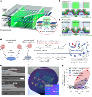
High-density displays are required for the development of virtual and augmented reality devices. However, increasing the pixel resolution can lead to higher electrical pixel crosstalk, primarily due to a shared hole transport layer. Here we show that a silicone-integrated small-molecule hole transport layer can be patterned at the wafer scale with microlithography to mitigate electrical pixel crosstalk. This provides high-density pixelation and improved performance of the hole transport layer itself. With this approach, we create high-fidelity micro-pattern arrays with a resolution of up to 10,062 pixels per inch on a six-inch wafer. The silicone-integrated small-molecule hole transport layer can effectively modulate charge balance within the emission layers, improving the luminance characteristics of organic light-emitting diodes. We also show that organic light-emitting diodes integrated with micro-patterned silicone-integrated small-molecule hole transport layers have a reduced electrical pixel crosstalk compared with organic light-emitting diodes with a typical hole transport layer. The robustness of small-molecule organic films can be increased by incorporating silicone blocks, allowing them to be patterned at high resolution, and used to make pixelated hole transport layers that reduce crosstalk in high-pixel-density displays.

减少电串扰的高分辨率有机发光二极管空穴传输层的微光刻技术
高密度显示器是开发虚拟现实和增强现实设备所必需的。然而,增加像素分辨率会导致更高的电像素串扰,这主要是由于共享空穴传输层。在这里,我们展示了硅集成的小分子空穴传输层可以在晶圆尺度上用微光刻技术进行图像化,以减轻电像素串扰。这提供了高密度的像素化,并提高了空穴传输层本身的性能。通过这种方法,我们在6英寸晶圆上创建了分辨率高达10062像素/英寸的高保真微图案阵列。有机硅集成的小分子空穴传输层可以有效地调节发射层内的电荷平衡,改善有机发光二极管的亮度特性。我们还表明,与具有典型空穴传输层的有机发光二极管相比,集成了微图像化硅集成小分子空穴传输层的有机发光二极管具有更少的电像元串扰。
本文章由计算机程序翻译,如有差异,请以英文原文为准。
求助全文
约1分钟内获得全文
求助全文
来源期刊
Nature Electronics
Engineering-Electrical and Electronic Engineering
CiteScore
47.50
自引率
2.30%
发文量
159
期刊介绍:
Nature Electronics is a comprehensive journal that publishes both fundamental and applied research in the field of electronics. It encompasses a wide range of topics, including the study of new phenomena and devices, the design and construction of electronic circuits, and the practical applications of electronics. In addition, the journal explores the commercial and industrial aspects of electronics research.
The primary focus of Nature Electronics is on the development of technology and its potential impact on society. The journal incorporates the contributions of scientists, engineers, and industry professionals, offering a platform for their research findings. Moreover, Nature Electronics provides insightful commentary, thorough reviews, and analysis of the key issues that shape the field, as well as the technologies that are reshaping society.
Like all journals within the prestigious Nature brand, Nature Electronics upholds the highest standards of quality. It maintains a dedicated team of professional editors and follows a fair and rigorous peer-review process. The journal also ensures impeccable copy-editing and production, enabling swift publication. Additionally, Nature Electronics prides itself on its editorial independence, ensuring unbiased and impartial reporting.
In summary, Nature Electronics is a leading journal that publishes cutting-edge research in electronics. With its multidisciplinary approach and commitment to excellence, the journal serves as a valuable resource for scientists, engineers, and industry professionals seeking to stay at the forefront of advancements in the field.
 求助内容:
求助内容: 应助结果提醒方式:


