Low-Cost Preparation of Wafer-Scale Au(111) Single Crystals for the Epitaxy of Two-Dimensional Layered Materials
IF 15.8
1区 材料科学
Q1 CHEMISTRY, MULTIDISCIPLINARY
引用次数: 0
Abstract
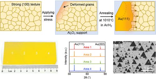
Single-crystal Au(111), renowned for its chemically inert surface, long-range “herringbone” reconstruction, and high electrical conductivity, has long served as an exemplary template in diverse fields, e.g., crystal epitaxy, electronics, and electrocatalysis. However, commercial Au(111) products are high-priced and limited to centimeter sizes, largely restricting their broad applications. Herein, a low-cost, high-reproducible method is developed to produce 4 in. Au(111) single crystals from commercial Au foils, via an abnormal grain growth process. This methodology involves the initial preparation of a (100)-textured Au polycrystalline foil, followed by the evolution and continuous expansion of an Au(111) abnormal grain through one-site stress loading and stress-relief annealing in an Ar/H2 atmosphere. Theoretical simulations indicate that stress/strain and high-temperature treatments in the H2 atmosphere induce an intermediate disordered state, facilitating the evolution from polycrystalline Au(100) foil to single-crystal Au(111) foil. Furthermore, the resulting Au(111) foils have been utilized as model substrates for the oriented growth of two-dimensional transition metal dichalcogenides and their heterostructures with graphene. This work hereby puts forward an effective approach for large-scale, cost-effective production of metal single crystals, potentially revolutionizing their applications across various fields, from materials sciences to electronics and catalysis.

求助全文
约1分钟内获得全文
求助全文
来源期刊

ACS Nano
工程技术-材料科学:综合
CiteScore
26.00
自引率
4.10%
发文量
1627
审稿时长
1.7 months
期刊介绍:
ACS Nano, published monthly, serves as an international forum for comprehensive articles on nanoscience and nanotechnology research at the intersections of chemistry, biology, materials science, physics, and engineering. The journal fosters communication among scientists in these communities, facilitating collaboration, new research opportunities, and advancements through discoveries. ACS Nano covers synthesis, assembly, characterization, theory, and simulation of nanostructures, nanobiotechnology, nanofabrication, methods and tools for nanoscience and nanotechnology, and self- and directed-assembly. Alongside original research articles, it offers thorough reviews, perspectives on cutting-edge research, and discussions envisioning the future of nanoscience and nanotechnology.
 求助内容:
求助内容: 应助结果提醒方式:


