Correlative Raman–Voltage Microscopy Revealing the Localized Structure–Stress Relationship in Silicon Solar Cells

IF 15.8 1区 材料科学 Q1 CHEMISTRY, MULTIDISCIPLINARY
ACS Nano Pub Date : 2025-01-24 DOI:10.1021/acsnano.4c13688
Tianyu Lan, Tianyi Zhao, Yan Liu, Jingyu Cao, Wenqi Li, Jie Yang, Xinyu Zhang, Yusheng Wang, Baoquan Sun
{"title":"Correlative Raman–Voltage Microscopy Revealing the Localized Structure–Stress Relationship in Silicon Solar Cells","authors":"Tianyu Lan, Tianyi Zhao, Yan Liu, Jingyu Cao, Wenqi Li, Jie Yang, Xinyu Zhang, Yusheng Wang, Baoquan Sun","doi":"10.1021/acsnano.4c13688","DOIUrl":null,"url":null,"abstract":"Knowledge of localized strain at the micrometer scale is essential for tailoring the electrical and mechanical properties of ongoing thinning of crystal silicon (c-Si) solar cells. Thinning c-Si wafers below 110 <i>μ</i>m are susceptible to cracking in manufacturing due to the nonuniform stress distribution at a micrometer region, necessitating a rigorous technique to reveal the localized stress distribution correlating with its device electrical output. In this context, a Raman microscopy integrated with a photovoltage mapping setup with high resolution to the submicrometer scale is developed to acquire correlative Raman–voltage of the localized physical properties at the microcracks on the rear side of c-Si solar cells. By integrating photoelectrical, mechanical, and theoretical simulations, we elucidated the evolution of the microcracks. The localized stresses cause significant electrical output degradation in c-Si solar cells. In addition, theoretical simulations and experimental characterization indicate that the etched rear side acts as a more intense stress concentrator, resulting in an asymmetrical stress distribution between the rear and front sides of c-Si solar cells. This finding provides valuable insights into the origin of microcracks in c-Si solar cells and serves as a metrology tool for microscale mapping of strain-engineered photovoltaic modules.","PeriodicalId":21,"journal":{"name":"ACS Nano","volume":"38 1","pages":""},"PeriodicalIF":15.8000,"publicationDate":"2025-01-24","publicationTypes":"Journal Article","fieldsOfStudy":null,"isOpenAccess":false,"openAccessPdf":"","citationCount":"0","resultStr":null,"platform":"Semanticscholar","paperid":null,"PeriodicalName":"ACS Nano","FirstCategoryId":"88","ListUrlMain":"https://doi.org/10.1021/acsnano.4c13688","RegionNum":1,"RegionCategory":"材料科学","ArticlePicture":[],"TitleCN":null,"AbstractTextCN":null,"PMCID":null,"EPubDate":"","PubModel":"","JCR":"Q1","JCRName":"CHEMISTRY, MULTIDISCIPLINARY","Score":null,"Total":0}
引用次数: 0

Abstract

Knowledge of localized strain at the micrometer scale is essential for tailoring the electrical and mechanical properties of ongoing thinning of crystal silicon (c-Si) solar cells. Thinning c-Si wafers below 110 μm are susceptible to cracking in manufacturing due to the nonuniform stress distribution at a micrometer region, necessitating a rigorous technique to reveal the localized stress distribution correlating with its device electrical output. In this context, a Raman microscopy integrated with a photovoltage mapping setup with high resolution to the submicrometer scale is developed to acquire correlative Raman–voltage of the localized physical properties at the microcracks on the rear side of c-Si solar cells. By integrating photoelectrical, mechanical, and theoretical simulations, we elucidated the evolution of the microcracks. The localized stresses cause significant electrical output degradation in c-Si solar cells. In addition, theoretical simulations and experimental characterization indicate that the etched rear side acts as a more intense stress concentrator, resulting in an asymmetrical stress distribution between the rear and front sides of c-Si solar cells. This finding provides valuable insights into the origin of microcracks in c-Si solar cells and serves as a metrology tool for microscale mapping of strain-engineered photovoltaic modules.
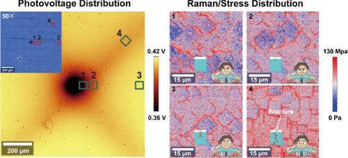
Abstract Image

求助全文
约1分钟内获得全文 求助全文
来源期刊
ACS Nano
ACS Nano 工程技术-材料科学:综合
CiteScore
26.00
自引率
4.10%
发文量
1627
审稿时长
1.7 months
期刊介绍: ACS Nano, published monthly, serves as an international forum for comprehensive articles on nanoscience and nanotechnology research at the intersections of chemistry, biology, materials science, physics, and engineering. The journal fosters communication among scientists in these communities, facilitating collaboration, new research opportunities, and advancements through discoveries. ACS Nano covers synthesis, assembly, characterization, theory, and simulation of nanostructures, nanobiotechnology, nanofabrication, methods and tools for nanoscience and nanotechnology, and self- and directed-assembly. Alongside original research articles, it offers thorough reviews, perspectives on cutting-edge research, and discussions envisioning the future of nanoscience and nanotechnology.
×
引用
GB/T 7714-2015
复制
MLA
复制
APA
复制
导出至
BibTeX EndNote RefMan NoteFirst NoteExpress
×
提示
您的信息不完整,为了账户安全,请先补充。
现在去补充
×
提示
您因"违规操作"
具体请查看互助需知
我知道了
×
提示
确定
请完成安全验证×
copy
已复制链接
快去分享给好友吧!
我知道了
右上角分享
点击右上角分享
0
联系我们:info@booksci.cn Book学术提供免费学术资源搜索服务,方便国内外学者检索中英文文献。致力于提供最便捷和优质的服务体验。 Copyright © 2023 布克学术 All rights reserved.
京ICP备2023020795号-1
ghs 京公网安备 11010802042870号
Book学术文献互助
Book学术文献互助群
群 号:481959085
Book学术官方微信