Ultranarrow Semiconductor WS2 Nanoribbon Field-Effect Transistors

IF 9.6 1区 材料科学 Q1 CHEMISTRY, MULTIDISCIPLINARY
Md. Anamul Hoque, Alexander Yu. Polyakov, Battulga Munkhbat, Konstantina Iordanidou, Abhay V. Agrawal, Andrew B. Yankovich, Sameer K. Mallik, Bing Zhao, Richa Mitra, Alexei Kalaboukhov, Eva Olsson, Sergey Kubatkin, Julia Wiktor, Samuel Lara Avila, Timur O. Shegai, Saroj P. Dash
{"title":"Ultranarrow Semiconductor WS2 Nanoribbon Field-Effect Transistors","authors":"Md. Anamul Hoque, Alexander Yu. Polyakov, Battulga Munkhbat, Konstantina Iordanidou, Abhay V. Agrawal, Andrew B. Yankovich, Sameer K. Mallik, Bing Zhao, Richa Mitra, Alexei Kalaboukhov, Eva Olsson, Sergey Kubatkin, Julia Wiktor, Samuel Lara Avila, Timur O. Shegai, Saroj P. Dash","doi":"10.1021/acs.nanolett.4c01076","DOIUrl":null,"url":null,"abstract":"Semiconducting transition metal dichalcogenides (TMDs) have attracted significant attention for their potential to develop high-performance, energy-efficient, and nanoscale electronic devices. Despite notable advancements in scaling down the gate and channel length of TMD field-effect transistors (FETs), the fabrication of sub-30 nm narrow channels and devices with atomic-scale edge control still poses challenges. Here, we demonstrate a crystallography-controlled nanostructuring technique to fabricate ultranarrow tungsten disulfide (WS<sub>2</sub>) nanoribbons as small as sub-10 nm in width. The WS<sub>2</sub> nanoribbon junctions having different widths display diodic current–voltage characteristics, providing a way to create and tune nanoscale device properties by controlling the size of the structures. The transport properties of the nanoribbon FETs are primarily governed by narrow channel effects, where the mobility in the narrow channels is limited by edge scattering. Our findings on nanoribbon devices hold potential for developing future-generation nanometer-scale van der Waals semiconductor-based devices and circuits.","PeriodicalId":53,"journal":{"name":"Nano Letters","volume":"57 1","pages":""},"PeriodicalIF":9.6000,"publicationDate":"2025-01-23","publicationTypes":"Journal Article","fieldsOfStudy":null,"isOpenAccess":false,"openAccessPdf":"","citationCount":"0","resultStr":null,"platform":"Semanticscholar","paperid":null,"PeriodicalName":"Nano Letters","FirstCategoryId":"88","ListUrlMain":"https://doi.org/10.1021/acs.nanolett.4c01076","RegionNum":1,"RegionCategory":"材料科学","ArticlePicture":[],"TitleCN":null,"AbstractTextCN":null,"PMCID":null,"EPubDate":"","PubModel":"","JCR":"Q1","JCRName":"CHEMISTRY, MULTIDISCIPLINARY","Score":null,"Total":0}
引用次数: 0

Abstract

Semiconducting transition metal dichalcogenides (TMDs) have attracted significant attention for their potential to develop high-performance, energy-efficient, and nanoscale electronic devices. Despite notable advancements in scaling down the gate and channel length of TMD field-effect transistors (FETs), the fabrication of sub-30 nm narrow channels and devices with atomic-scale edge control still poses challenges. Here, we demonstrate a crystallography-controlled nanostructuring technique to fabricate ultranarrow tungsten disulfide (WS2) nanoribbons as small as sub-10 nm in width. The WS2 nanoribbon junctions having different widths display diodic current–voltage characteristics, providing a way to create and tune nanoscale device properties by controlling the size of the structures. The transport properties of the nanoribbon FETs are primarily governed by narrow channel effects, where the mobility in the narrow channels is limited by edge scattering. Our findings on nanoribbon devices hold potential for developing future-generation nanometer-scale van der Waals semiconductor-based devices and circuits.

Abstract Image

超狭半导体WS2纳米带场效应晶体管
半导体过渡金属二硫族化合物(TMDs)因其具有开发高性能、高能效和纳米级电子器件的潜力而受到广泛关注。尽管在缩小TMD场效应晶体管(fet)的栅极和沟道长度方面取得了显著进展,但制造低于30纳米的窄沟道和具有原子尺度边缘控制的器件仍然面临挑战。在这里,我们展示了一种晶体学控制的纳米结构技术,可以制造宽度小于10纳米的超窄二硫化钨(WS2)纳米带。具有不同宽度的WS2纳米带结显示二极管电流-电压特性,提供了一种通过控制结构尺寸来创建和调整纳米级器件特性的方法。纳米带场效应管的输运特性主要受窄通道效应的影响,窄通道中的迁移率受边缘散射的限制。我们在纳米带器件上的发现为开发下一代纳米尺度范德华半导体器件和电路提供了潜力。
本文章由计算机程序翻译,如有差异,请以英文原文为准。
求助全文
约1分钟内获得全文 求助全文
来源期刊
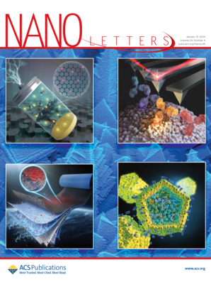
Nano Letters
Nano Letters 工程技术-材料科学:综合
CiteScore
16.80
自引率
2.80%
发文量
1182
审稿时长
1.4 months
期刊介绍: Nano Letters serves as a dynamic platform for promptly disseminating original results in fundamental, applied, and emerging research across all facets of nanoscience and nanotechnology. A pivotal criterion for inclusion within Nano Letters is the convergence of at least two different areas or disciplines, ensuring a rich interdisciplinary scope. The journal is dedicated to fostering exploration in diverse areas, including: - Experimental and theoretical findings on physical, chemical, and biological phenomena at the nanoscale - Synthesis, characterization, and processing of organic, inorganic, polymer, and hybrid nanomaterials through physical, chemical, and biological methodologies - Modeling and simulation of synthetic, assembly, and interaction processes - Realization of integrated nanostructures and nano-engineered devices exhibiting advanced performance - Applications of nanoscale materials in living and environmental systems Nano Letters is committed to advancing and showcasing groundbreaking research that intersects various domains, fostering innovation and collaboration in the ever-evolving field of nanoscience and nanotechnology.
×
引用
GB/T 7714-2015
复制
MLA
复制
APA
复制
导出至
BibTeX EndNote RefMan NoteFirst NoteExpress
×
提示
您的信息不完整,为了账户安全,请先补充。
现在去补充
×
提示
您因"违规操作"
具体请查看互助需知
我知道了
×
提示
确定
请完成安全验证×
copy
已复制链接
快去分享给好友吧!
我知道了
右上角分享
点击右上角分享
0
联系我们:info@booksci.cn Book学术提供免费学术资源搜索服务,方便国内外学者检索中英文文献。致力于提供最便捷和优质的服务体验。 Copyright © 2023 布克学术 All rights reserved.
京ICP备2023020795号-1
ghs 京公网安备 11010802042870号
Book学术文献互助
Book学术文献互助群
群 号:481959085
Book学术官方微信