Improved Conductivity of 2D Perovskite Capping Layer for Realizing High-Performance 3D/2D Heterostructured Hole Transport Layer-Free Perovskite Photovoltaics
IF 16
1区 材料科学
Q1 CHEMISTRY, MULTIDISCIPLINARY
引用次数: 0
Abstract
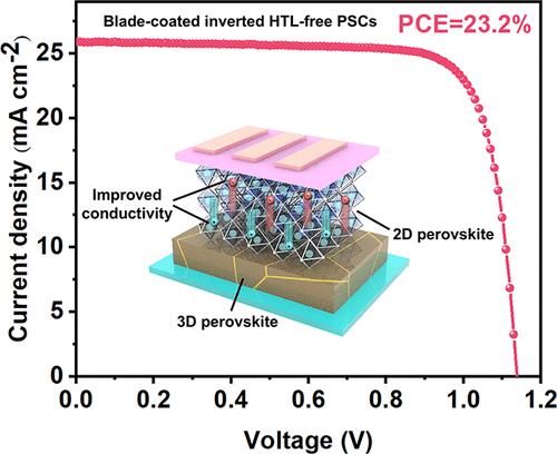
Perovskite solar cells (PSCs) have emerged as low-cost photovoltaic representatives. Constructing three-dimensional (3D)/two-dimensional (2D) perovskite heterostructures has been shown to effectively enhance the efficiency and stability of PSCs. However, further enhancement of device performance is still largely limited by inferior conductivity of the 2D perovskite capping layer and its mismatched energy level with the 3D perovskite layer. Here, we developed an effective surface modification strategy via synergically incorporating inorganic high valence-state niobium ion (Nb5+) metal dopants and organic ammonium halide salts to in situ construct a high-quality 2D perovskite capping layer on top of the underlying 3D perovskite layer. As a result, the conductivity of the 2D perovskite capping layer was effectively enhanced by 43%, the energy barrier between 3D and 2D perovskite layers was favorably reduced, and the built-in electric field of the 3D/2D heterostructured perovskite stacks has been enlarged. In addition, the 2D perovskite capping layer also effectively reduced the defect densities by up to 29%, as verified by the space-charge-limited-current (SCLC) tests. Benefiting from the facilitated charge extraction and suppressed non-radiative recombination, the blade-coated hole transport layer-free PSCs based on this optimized 3D/2D heterostructured perovskite film achieved an efficiency of 23.2%, ∼19% higher than that of the control device (19.5%), which represented one of the best-performing PSCs with simplified device architecture fabricated via a scalable fabrication technique. The modified 3D/2D perovskite-based device also exhibited improved operational stability.
提高二维钙钛矿封盖层导电性,实现高性能3D/2D异质结构空穴传输无层钙钛矿光伏
钙钛矿太阳能电池(PSCs)已成为低成本光伏电池的代表。构建三维(3D)/二维(2D)钙钛矿异质结构已被证明可以有效提高PSCs的效率和稳定性。然而,由于二维钙钛矿封盖层电导率较低,且与三维钙钛矿封盖层的能级不匹配,器件性能的进一步提升在很大程度上仍然受到限制。在这里,我们开发了一种有效的表面改性策略,通过协同结合无机高价态铌离子(Nb5+)金属掺杂剂和有机卤化铵盐,在底层的3D钙钛矿层上原位构建高质量的2D钙钛矿覆盖层。结果表明,2D钙钛矿覆盖层的电导率有效提高了43%,有利于降低3D和2D钙钛矿层之间的能垒,扩大了3D/2D异质结构钙钛矿堆叠的内置电场。此外,通过空间电荷限流(SCLC)测试证实,2D钙钛矿封盖层还有效地将缺陷密度降低了29%。得益于易于电荷提取和抑制非辐射复合,基于这种优化的3D/2D异质钙钛矿膜的叶片涂层空穴传输无层PSCs的效率达到23.2%,比控制器件(19.5%)高出19%,这是通过可扩展的制造技术制造的简化器件结构的性能最好的PSCs之一。改良的3D/2D钙钛矿基器件也表现出更好的操作稳定性。
本文章由计算机程序翻译,如有差异,请以英文原文为准。
求助全文
约1分钟内获得全文
求助全文
来源期刊

ACS Nano
工程技术-材料科学:综合
CiteScore
26.00
自引率
4.10%
发文量
1627
审稿时长
1.7 months
期刊介绍:
ACS Nano, published monthly, serves as an international forum for comprehensive articles on nanoscience and nanotechnology research at the intersections of chemistry, biology, materials science, physics, and engineering. The journal fosters communication among scientists in these communities, facilitating collaboration, new research opportunities, and advancements through discoveries. ACS Nano covers synthesis, assembly, characterization, theory, and simulation of nanostructures, nanobiotechnology, nanofabrication, methods and tools for nanoscience and nanotechnology, and self- and directed-assembly. Alongside original research articles, it offers thorough reviews, perspectives on cutting-edge research, and discussions envisioning the future of nanoscience and nanotechnology.
 求助内容:
求助内容: 应助结果提醒方式:


