Interfacial Elemental Analysis of Slanted Edge-Contacted Monolayer MoS2 Transistors via Directionally Angled Etching
IF 15.8
1区 材料科学
Q1 CHEMISTRY, MULTIDISCIPLINARY
引用次数: 0
Abstract
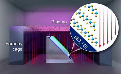
Edge contacts offer a significant advantage for enhancing the performance of semiconducting transition metal dichalcogenide (TMDC) devices by interfacing with the metallic contacts on the lateral side, which allows the encapsulation of all of the channel material. However, despite intense research, the fabrication of feasible electrical edge contacts to TMDCs to improve device performance remains a great challenge, as interfacial chemical characterization via conventional methods is lacking. A major bottleneck in explicitly understanding the chemical and electronic properties of the edge contact at the metal–two-dimensional (2D) semiconductor interface is the small cross section when characterizing nominally one-dimensional edge contacts. Here, we demonstrate a directional angled etching technique that enables the characterization of the interfacial chemistry at the metal–MoS2 junction when in an edge-contact configuration. The slanted edge structure provides a substantial cross section for elemental analysis of the edge contact by conventional X-ray photoemission spectroscopy, in which a simple chemical environment and sharp interface were revealed. Facilitated by the well-characterized contact interface, we realized slanted edge-contacted monolayer MoS2 transistors encapsulated by hexagonal boron nitride. The transport characteristics and photoluminescence of these transistors allowed us to attribute the efficient carrier injection to direct and Fowler–Nordheim tunneling, validating the distinct Au–MoS2 interface. The established method represents a viable approach to fabricating edge contacts with encapsulated 2D material devices, which is crucial for both the fundamental study of 2D materials and high-performance electronic applications.

斜边接触MoS2单层晶体管的定向角刻蚀界面元素分析
边缘触点通过与侧面的金属触点连接,可以封装所有通道材料,从而为提高半导体过渡金属二硫化物(TMDC)器件的性能提供了显著的优势。然而,尽管进行了大量的研究,但由于缺乏通过传统方法进行界面化学表征,制造可行的TMDCs电边缘触点以提高器件性能仍然是一个巨大的挑战。明确理解金属-二维(2D)半导体界面边缘接触的化学和电子特性的主要瓶颈是表征名义上一维边缘接触时的小截面。在这里,我们展示了一种定向角度蚀刻技术,该技术能够表征金属- mos2结在边缘接触配置时的界面化学。倾斜的边缘结构为传统x射线光谱学分析边缘接触提供了大量的横截面,揭示了简单的化学环境和尖锐的界面。利用表征良好的接触界面,我们实现了六方氮化硼封装的斜边接触单层MoS2晶体管。这些晶体管的输运特性和光致发光使我们能够将有效的载流子注入归因于直接和Fowler-Nordheim隧道,验证了独特的Au-MoS2界面。所建立的方法代表了用封装的二维材料器件制造边缘接触的可行方法,这对于二维材料的基础研究和高性能电子应用都至关重要。
本文章由计算机程序翻译,如有差异,请以英文原文为准。
求助全文
约1分钟内获得全文
求助全文
来源期刊

ACS Nano
工程技术-材料科学:综合
CiteScore
26.00
自引率
4.10%
发文量
1627
审稿时长
1.7 months
期刊介绍:
ACS Nano, published monthly, serves as an international forum for comprehensive articles on nanoscience and nanotechnology research at the intersections of chemistry, biology, materials science, physics, and engineering. The journal fosters communication among scientists in these communities, facilitating collaboration, new research opportunities, and advancements through discoveries. ACS Nano covers synthesis, assembly, characterization, theory, and simulation of nanostructures, nanobiotechnology, nanofabrication, methods and tools for nanoscience and nanotechnology, and self- and directed-assembly. Alongside original research articles, it offers thorough reviews, perspectives on cutting-edge research, and discussions envisioning the future of nanoscience and nanotechnology.
 求助内容:
求助内容: 应助结果提醒方式:


