Design of an Atomic Layer-Deposited In2O3/Ga2O3 Channel Structure for High-Performance Thin-Film Transistors
IF 8.3
2区 材料科学
Q1 MATERIALS SCIENCE, MULTIDISCIPLINARY
引用次数: 0
Abstract
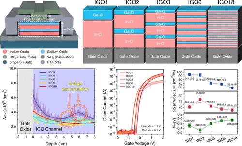
For potential application in advanced memory devices such as dynamic random-access memory (DRAM) or NAND flash, nanolaminated indium oxide (In–O) and gallium oxide (Ga–O) films with five different vertical cation distributions were grown and investigated by using a plasma-enhanced atomic layer deposition (PEALD) process. Specifically, this study provides an in-depth examination of how the control of individual layer thicknesses in the nanolaminated (NL) IGO structure impacts not only the physical and chemical properties of the thin film but also the overall device performance. To eliminate the influence of the cation composition ratio and overall thickness on the IGO thin film, these parameters were held constant across all conditions. Thin-film transistors (TFTs) with a homogeneous In0.72Ga0.29Ox channel layer (referred to as IGO18) exhibited a reasonable field-effect mobility (μFE) of 58.1 cm2/(V s) and ION/OFF ratio of >108. A significant improvement (∼94.1 cm2/(V s)) in μFE was observed for TFTs with an In2O3/Ga2O3 heterojunction stack (referred to as IGO1). Because the channel layers of both devices had an identical average cation composition and physical thickness, the superior performance of the latter can be attributed to the emergence of a quasi-two-dimensional electron gas (2DEG) and the attainment of high-quality crystallinity. This study underscores the criticality of supercycle duty design to prevent cation intermixing, enabling the exploitation of the 2DEG effect in high-performance oxide TFTs for memory device applications.

高性能薄膜晶体管用原子层沉积In2O3/Ga2O3通道结构设计
为了在动态随机存取存储器(DRAM)或NAND闪存等先进存储设备中的潜在应用,采用等离子体增强原子层沉积(PEALD)工艺,生长并研究了具有五种不同垂直阳离子分布的纳米层化氧化铟(in - o)和氧化镓(Ga-O)薄膜。具体来说,本研究深入研究了纳米层化(NL) IGO结构中单个层厚度的控制如何影响薄膜的物理和化学性质,以及整体器件性能。为了消除阳离子组成比和总厚度对IGO薄膜的影响,这些参数在所有条件下都保持不变。具有均匀In0.72Ga0.29Ox沟道层(简称IGO18)的薄膜晶体管(TFTs)的场效应迁移率(μFE)为58.1 cm2/(V s),离子/OFF比为108。对于具有In2O3/Ga2O3异质结堆叠(称为IGO1)的tft,观察到μFE的显著改善(~ 94.1 cm2/(V s))。由于两种器件的通道层具有相同的平均阳离子组成和物理厚度,后者的优越性能可归因于准二维电子气体(2DEG)的出现和高质量结晶度的实现。该研究强调了防止阳离子混合的超循环负载设计的重要性,从而能够在用于存储器件的高性能氧化物tft中利用2DEG效应。
本文章由计算机程序翻译,如有差异,请以英文原文为准。
求助全文
约1分钟内获得全文
求助全文
来源期刊

ACS Applied Materials & Interfaces
工程技术-材料科学:综合
CiteScore
16.00
自引率
6.30%
发文量
4978
审稿时长
1.8 months
期刊介绍:
ACS Applied Materials & Interfaces is a leading interdisciplinary journal that brings together chemists, engineers, physicists, and biologists to explore the development and utilization of newly-discovered materials and interfacial processes for specific applications. Our journal has experienced remarkable growth since its establishment in 2009, both in terms of the number of articles published and the impact of the research showcased. We are proud to foster a truly global community, with the majority of published articles originating from outside the United States, reflecting the rapid growth of applied research worldwide.
 求助内容:
求助内容: 应助结果提醒方式:


