Capacitorless Dynamic Random Access Memory with 2D Transistors by One-Step Transfer of van der Waals Dielectrics and Electrodes
IF 15.8
1区 材料科学
Q1 CHEMISTRY, MULTIDISCIPLINARY
引用次数: 0
Abstract
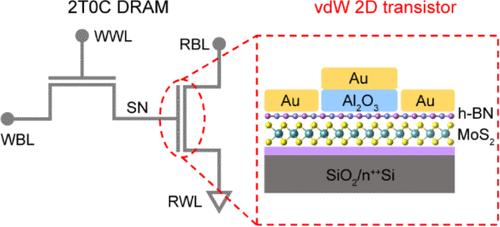
Dynamic random access memory (DRAM) has been a cornerstone of modern computing, but it faces challenges as technology scales down, particularly due to the mismatch between reduced storage capacitance and increasing OFF current. The capacitorless 2T0C DRAM architecture is recognized for its potential to offer superior area efficiency and reduced refresh rate requirements by eliminating the traditional capacitor. The exploration of two-dimensional (2D) materials further enhances scaling possibilities, though the absence of dangling bonds complicates the deposition of high-quality dielectrics. Here, we present a hexagonal boron nitride (h-BN)-assisted process for one-step transfer of van der Waals dielectrics and electrodes in 2D transistors with clean interfaces. The transferred aluminum oxide (Al2O3), formed by oxidizing aluminum (Al), exhibits exceptional flatness and uniformity, preserving the intrinsic properties of the 2D semiconductors without introducing doping effects. The MoS2 transistor exhibits an extremely low interface trap density of about 3 × 1011 cm–2 eV–1 and a leakage current density down to 10–7 A cm–2, which enables effective charge storage at the gate stack. This method allows for the simultaneous fabrication of two damage-free MoS2 transistors to form a capacitorless 2T0C DRAM cell, enhancing compatibility with 2D materials. The ultralow leakage current optimizes data retention and power efficiency. The fabricated 2T0C DRAM exhibits a rapid write speed of 20 ns, long data retention exceeding 1,000 s, and low energy consumption of approximately 0.2 fJ per write operation. Additionally, it demonstrates 3-bit storage capability and exceptional stability across numerous write/erase cycles.

范德华电介质和电极一步转移二维晶体管无电容动态随机存取存储器
动态随机存取存储器(DRAM)一直是现代计算的基石,但随着技术的缩小,它面临着挑战,特别是由于存储电容减少和OFF电流增加之间的不匹配。无电容2T0C DRAM架构因其消除传统电容而具有卓越的面积效率和降低刷新率要求的潜力而得到认可。二维(2D)材料的探索进一步提高了缩放的可能性,尽管悬空键的缺失使高质量电介质的沉积变得复杂。在这里,我们提出了一种六方氮化硼(h-BN)辅助工艺,用于在具有清洁界面的二维晶体管中一步转移范德华电介质和电极。由铝(Al)氧化形成的转移氧化铝(Al2O3)表现出优异的平整度和均匀性,在不引入掺杂效应的情况下保持了二维半导体的固有特性。MoS2晶体管具有极低的界面阱密度,约为3 × 1011 cm-2 eV-1,漏电流密度低至10-7 a cm-2,这使得栅极堆栈能够有效地存储电荷。该方法允许同时制造两个无损伤的MoS2晶体管,以形成无电容的2T0C DRAM单元,增强与2D材料的兼容性。超低漏电流优化数据保留和电源效率。所制备的2T0C DRAM具有20 ns的快速写入速度,超过1,000 s的长数据保留时间,每次写入操作的能耗约为0.2 fJ。此外,它还展示了3位存储能力和跨多个写/擦除周期的卓越稳定性。
本文章由计算机程序翻译,如有差异,请以英文原文为准。
求助全文
约1分钟内获得全文
求助全文
来源期刊

ACS Nano
工程技术-材料科学:综合
CiteScore
26.00
自引率
4.10%
发文量
1627
审稿时长
1.7 months
期刊介绍:
ACS Nano, published monthly, serves as an international forum for comprehensive articles on nanoscience and nanotechnology research at the intersections of chemistry, biology, materials science, physics, and engineering. The journal fosters communication among scientists in these communities, facilitating collaboration, new research opportunities, and advancements through discoveries. ACS Nano covers synthesis, assembly, characterization, theory, and simulation of nanostructures, nanobiotechnology, nanofabrication, methods and tools for nanoscience and nanotechnology, and self- and directed-assembly. Alongside original research articles, it offers thorough reviews, perspectives on cutting-edge research, and discussions envisioning the future of nanoscience and nanotechnology.
 求助内容:
求助内容: 应助结果提醒方式:


