A mass transfer technology for high-density two-dimensional device integration
IF 33.7
1区 工程技术
Q1 ENGINEERING, ELECTRICAL & ELECTRONIC
引用次数: 0
Abstract
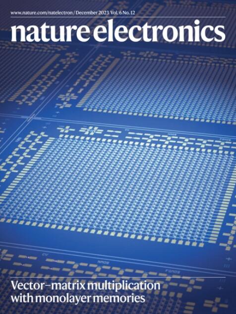
The large-area transfer of two-dimensional (2D) materials from their growth substrate is crucial for electronic device integration. However, it is easy to damage sub-1-nm thick materials, and existing transfer methods typically involve a trade-off in terms of lateral size, quality and accuracy. Here we report a mass transfer printing technology that uses a polydimethylsiloxane stamp patterned with precisely arranged micro-posts to gently transfer wafer-level 2D arrays and to stack van der Waals heterostructure arrays. After the stamp is brought into contact with the 2D material, an ethanol–water solution is added, which penetrates the 2D material–growth substrate interface between the non-contact regions of the stamp and causes the film to delaminate. We use the approach to transfer a 2-inch (~5 cm) monolayer molybdenum disulfide film containing more than 1,000,000 arrays with lateral dimensions of 20 × 20 µm2, a density of 62,500 arrays per cm2 and a yield of 99% in a single operation. Integrated 2D transistors with different device architectures created with the technology show a device yield of around 97.9% (back gate) and nearly damage-free electrical properties (top and bottom gate). We also develop a capillary force-assisted transfer model to explain the rapid transfer mechanism. Using a polymer stamp with a period arrangement of micro-posts on its surface and a high surface tension liquid, two-dimensional material films can be patterned and transferred on a large-scale with high yield.


高密度二维器件集成传质技术
从生长基底大面积转移二维(2D)材料对于电子设备集成至关重要。然而,1 纳米以下厚度的材料很容易损坏,而且现有的转移方法通常需要在横向尺寸、质量和精度方面进行权衡。在此,我们报告了一种大规模转移印刷技术,该技术采用聚二甲基硅氧烷印章,印章上图案为精确排列的微柱,可平缓转移晶圆级二维阵列,并堆叠范德华异质结构阵列。在印章与二维材料接触后,加入乙醇-水溶液,该溶液会渗入印章非接触区域之间的二维材料-生长基底界面,并导致薄膜分层。我们使用这种方法转移了一个 2 英寸(约 5 厘米)的单层二硫化钼薄膜,其中包含超过 1,000,000 个阵列,横向尺寸为 20 × 20 µm2,密度为每平方厘米 62,500 个阵列,单次操作良率为 99%。利用该技术制造的具有不同器件结构的集成二维晶体管显示出约 97.9% 的器件良率(背栅)和几乎无损坏的电气性能(顶栅和底栅)。我们还开发了一个毛细管力辅助转移模型来解释快速转移机制。
本文章由计算机程序翻译,如有差异,请以英文原文为准。
求助全文
约1分钟内获得全文
求助全文
来源期刊

Nature Electronics
Engineering-Electrical and Electronic Engineering
CiteScore
47.50
自引率
2.30%
发文量
159
期刊介绍:
Nature Electronics is a comprehensive journal that publishes both fundamental and applied research in the field of electronics. It encompasses a wide range of topics, including the study of new phenomena and devices, the design and construction of electronic circuits, and the practical applications of electronics. In addition, the journal explores the commercial and industrial aspects of electronics research.
The primary focus of Nature Electronics is on the development of technology and its potential impact on society. The journal incorporates the contributions of scientists, engineers, and industry professionals, offering a platform for their research findings. Moreover, Nature Electronics provides insightful commentary, thorough reviews, and analysis of the key issues that shape the field, as well as the technologies that are reshaping society.
Like all journals within the prestigious Nature brand, Nature Electronics upholds the highest standards of quality. It maintains a dedicated team of professional editors and follows a fair and rigorous peer-review process. The journal also ensures impeccable copy-editing and production, enabling swift publication. Additionally, Nature Electronics prides itself on its editorial independence, ensuring unbiased and impartial reporting.
In summary, Nature Electronics is a leading journal that publishes cutting-edge research in electronics. With its multidisciplinary approach and commitment to excellence, the journal serves as a valuable resource for scientists, engineers, and industry professionals seeking to stay at the forefront of advancements in the field.
 求助内容:
求助内容: 应助结果提醒方式:


