Selenium Interface Layers Boost High Mobility and Switch Ratios in van der Waals Electronics
IF 9.6
1区 材料科学
Q1 CHEMISTRY, MULTIDISCIPLINARY
引用次数: 0
Abstract
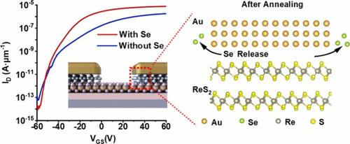
Achieving high mobility while minimizing off-current and static power consumption is critical for applications of two-dimensional field-effect transistors. Herein, a selenium (Se) sacrificial layer is introduced between the rhenium sulfide (ReS2) semiconductor and source/drain electrode. With the Se layer and postannealing process, the ReS2 transistor significantly decreases the off-state current with a substantial increase in the on-state current density. Notably, the mobility reaches 237 cm2 V–1 s–1, which is accompanied by an extraordinary current on/off ratio of 1011 at 7 K. The theoretical calculations and noise analysis show that the improvement in device performance is ascribed to the Se protective layer, which effectively shields the semiconductor from direct exposure to high-energy metal particles, reducing the Schottky barrier and the number of defect states at the interface. Finally, Se sacrificial ReS2 transistor-based versatile logic circuits including NAND and NOR logic are executed, which can be widely applied in integrated circuits.

硒界面层提高了范德华电子的高迁移率和开关比
实现高迁移率,同时最大限度地减少非电流和静态功耗是二维场效应晶体管应用的关键。本文在硫化铼(ReS2)半导体和源极/漏极之间引入硒(Se)牺牲层。通过Se层和后电印工艺,ReS2晶体管显着降低了断开状态电流,同时大幅增加了导通状态电流密度。值得注意的是,迁移率达到237 cm2 V-1 s-1,伴随着7 K时1011的异常电流开/关比。理论计算和噪声分析表明,器件性能的提高归因于Se保护层,它有效地屏蔽了半导体免受高能金属粒子的直接暴露,减少了肖特基势垒和界面缺陷态的数量。最后,设计了基于Se牺牲型ReS2晶体管的通用逻辑电路,包括NAND和NOR逻辑,可广泛应用于集成电路中。
本文章由计算机程序翻译,如有差异,请以英文原文为准。
求助全文
约1分钟内获得全文
求助全文
来源期刊

Nano Letters
工程技术-材料科学:综合
CiteScore
16.80
自引率
2.80%
发文量
1182
审稿时长
1.4 months
期刊介绍:
Nano Letters serves as a dynamic platform for promptly disseminating original results in fundamental, applied, and emerging research across all facets of nanoscience and nanotechnology. A pivotal criterion for inclusion within Nano Letters is the convergence of at least two different areas or disciplines, ensuring a rich interdisciplinary scope. The journal is dedicated to fostering exploration in diverse areas, including:
- Experimental and theoretical findings on physical, chemical, and biological phenomena at the nanoscale
- Synthesis, characterization, and processing of organic, inorganic, polymer, and hybrid nanomaterials through physical, chemical, and biological methodologies
- Modeling and simulation of synthetic, assembly, and interaction processes
- Realization of integrated nanostructures and nano-engineered devices exhibiting advanced performance
- Applications of nanoscale materials in living and environmental systems
Nano Letters is committed to advancing and showcasing groundbreaking research that intersects various domains, fostering innovation and collaboration in the ever-evolving field of nanoscience and nanotechnology.
 求助内容:
求助内容: 应助结果提醒方式:


