Hybrid-Size Quantum Dots in Hole Transport Layer Depress Dark Current Density of Short-Wave Infrared Photodetectors

IF 6.5 1区 物理与天体物理 Q1 MATERIALS SCIENCE, MULTIDISCIPLINARY
Simin Chen, Huaying Zhong, Xiao Wang, Guangjiu Pan, Haodong Tang, Fan Fang, Jiufeng Wu, Weichao Wang, Lihai Xu, Jun Tang, Junjie Hao, Keyu Zheng, Dan Wu, Zeguo Tang, Lei Zhang, Leifeng Cao, Peter Müller-Buschbaum, Kai Wang, Wei Chen
{"title":"Hybrid-Size Quantum Dots in Hole Transport Layer Depress Dark Current Density of Short-Wave Infrared Photodetectors","authors":"Simin Chen, Huaying Zhong, Xiao Wang, Guangjiu Pan, Haodong Tang, Fan Fang, Jiufeng Wu, Weichao Wang, Lihai Xu, Jun Tang, Junjie Hao, Keyu Zheng, Dan Wu, Zeguo Tang, Lei Zhang, Leifeng Cao, Peter Müller-Buschbaum, Kai Wang, Wei Chen","doi":"10.1021/acsphotonics.4c01864","DOIUrl":null,"url":null,"abstract":"PbS quantum dots (QDs) are promising materials for low-cost short-wave infrared (SWIR) photodetection and imaging applications, owing to their unique optical properties and tunable bandgap. High-performance photodiodes rely on thiol-treated small PbS QDs as the hole transport layer (HTL) due to their suitable band alignment, but they face challenges such as crack formation, which increases dark currents. We develop a crack-free HTL by mixing small-size and large-size QDs. Grazing incidence small-angle X-ray scattering data confirms that the hybrid-size QD HTL is more homogeneous and denser than that made from monosize QDs. Photophysical studies show optimized charge carrier dynamics and energy transfer in the hybrid-size QDs, compared to monosize QDs. The devices based on the hybrid-size QD HTL exhibit a significantly reduced dark current density (392 nA/cm<sup>2</sup>). Additionally, they show high device performance, including a responsivity of 0.65 A/W, detectivity of 2.4 × 10<sup>12</sup> Jones, and an external quantum efficiency of 65% in the SWIR region, paving the way for high-performance QD-based SWIR photodetectors.","PeriodicalId":23,"journal":{"name":"ACS Photonics","volume":"72 1","pages":""},"PeriodicalIF":6.5000,"publicationDate":"2025-01-02","publicationTypes":"Journal Article","fieldsOfStudy":null,"isOpenAccess":false,"openAccessPdf":"","citationCount":"0","resultStr":null,"platform":"Semanticscholar","paperid":null,"PeriodicalName":"ACS Photonics","FirstCategoryId":"101","ListUrlMain":"https://doi.org/10.1021/acsphotonics.4c01864","RegionNum":1,"RegionCategory":"物理与天体物理","ArticlePicture":[],"TitleCN":null,"AbstractTextCN":null,"PMCID":null,"EPubDate":"","PubModel":"","JCR":"Q1","JCRName":"MATERIALS SCIENCE, MULTIDISCIPLINARY","Score":null,"Total":0}
引用次数: 0

Abstract

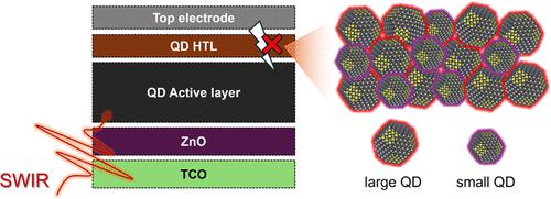
PbS quantum dots (QDs) are promising materials for low-cost short-wave infrared (SWIR) photodetection and imaging applications, owing to their unique optical properties and tunable bandgap. High-performance photodiodes rely on thiol-treated small PbS QDs as the hole transport layer (HTL) due to their suitable band alignment, but they face challenges such as crack formation, which increases dark currents. We develop a crack-free HTL by mixing small-size and large-size QDs. Grazing incidence small-angle X-ray scattering data confirms that the hybrid-size QD HTL is more homogeneous and denser than that made from monosize QDs. Photophysical studies show optimized charge carrier dynamics and energy transfer in the hybrid-size QDs, compared to monosize QDs. The devices based on the hybrid-size QD HTL exhibit a significantly reduced dark current density (392 nA/cm2). Additionally, they show high device performance, including a responsivity of 0.65 A/W, detectivity of 2.4 × 10¹² Jones, and an external quantum efficiency of 65% in the SWIR region, paving the way for high-performance QD-based SWIR photodetectors.
Abstract Image

空穴传输层中混合尺寸量子点对短波红外探测器暗电流密度的影响
PbS量子点由于其独特的光学特性和可调谐的带隙,是低成本短波红外(SWIR)光探测和成像应用的有前途的材料。高性能光电二极管依赖于巯基处理的小PbS量子点作为空穴传输层(HTL),因为它们具有合适的能带排列,但它们面临着诸如裂纹形成等挑战,这会增加暗电流。我们通过混合小尺寸和大尺寸量子点来开发无裂纹的html。掠入射小角度x射线散射数据证实,混合尺寸量子点HTL比单尺寸量子点HTL更均匀,密度更大。光物理研究表明,与单尺寸量子点相比,混合尺寸量子点的载流子动力学和能量传递得到了优化。基于混合尺寸QD HTL的器件显示出明显降低的暗电流密度(392 nA/cm2)。此外,它们还具有较高的器件性能,包括响应率为0.65 a /W,探测率为2.4 × 1012 Jones, SWIR区域的外部量子效率为65%,为高性能基于qd的SWIR光电探测器铺平了道路。
本文章由计算机程序翻译,如有差异,请以英文原文为准。
求助全文
约1分钟内获得全文 求助全文
来源期刊
ACS Photonics
ACS Photonics NANOSCIENCE & NANOTECHNOLOGY-MATERIALS SCIENCE, MULTIDISCIPLINARY
CiteScore
11.90
自引率
5.70%
发文量
438
审稿时长
2.3 months
期刊介绍: Published as soon as accepted and summarized in monthly issues, ACS Photonics will publish Research Articles, Letters, Perspectives, and Reviews, to encompass the full scope of published research in this field.
×
引用
GB/T 7714-2015
复制
MLA
复制
APA
复制
导出至
BibTeX EndNote RefMan NoteFirst NoteExpress
×
提示
您的信息不完整,为了账户安全,请先补充。
现在去补充
×
提示
您因"违规操作"
具体请查看互助需知
我知道了
×
提示
确定
请完成安全验证×
copy
已复制链接
快去分享给好友吧!
我知道了
右上角分享
点击右上角分享
0
联系我们:info@booksci.cn Book学术提供免费学术资源搜索服务,方便国内外学者检索中英文文献。致力于提供最便捷和优质的服务体验。 Copyright © 2023 布克学术 All rights reserved.
京ICP备2023020795号-1
ghs 京公网安备 11010802042870号
Book学术文献互助
Book学术文献互助群
群 号:481959085
Book学术官方微信