P-Type Vertical FETs Realized by Using Fermi-Level Pinning-Free 2D Metallic Electrodes
IF 9.6
1区 材料科学
Q1 CHEMISTRY, MULTIDISCIPLINARY
引用次数: 0
Abstract
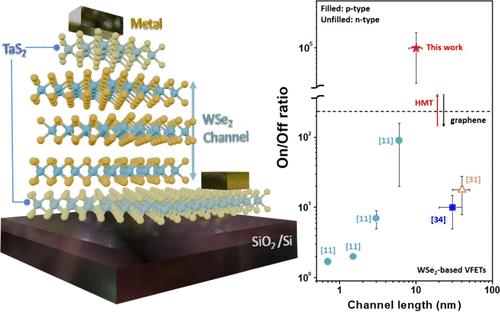
In two-dimensional (2D) nanomaterial electronics, vertical field-effect transistors (VFETs), where charges flow perpendicular to the channel materials, hold promise due to the ease of forming ultrashort channel lengths by utilizing the thinness of 2D materials. However, the poor performance of p-type VFET arises from the lack of a gate-field-penetrating electrode with suitable work functions, which is essential for VFET operation. This motivated us to replace graphene (work function of ∼4.5 eV) with a high-work-function electrode to achieve the desired VFET characteristics. In this study, we demonstrate that WSe2-based p-type VFETs with a high on/off ratio of ∼105 can be realized using van-der-Waals contacts formed with high-work-function 2D metals (i.e., 2H-TaS2, NbSe2, and NbS2), which form a p-type ohmic contact to the WSe2 channel by suppressing Fermi-level pinning. Furthermore, we successfully fabricate a 2D metal-incorporating pseudocomplementary FET structure, demonstrating a great potential to significantly reduce the scaling factor by dense structure and vertical operation.

用费米级无钉钉二维金属电极实现p型垂直场效应管
在二维(2D)纳米材料电子学中,垂直场效应晶体管(vfet),其中电荷垂直于通道材料流动,由于利用二维材料的薄度易于形成超短通道长度,因此前景广阔。然而,p型场效应管性能不佳的原因是缺乏具有合适功函数的栅场穿透电极,这是场效应管工作所必需的。这促使我们用高功函数电极取代石墨烯(功函数为~ 4.5 eV),以实现所需的VFET特性。在这项研究中,我们证明了基于WSe2的p型vfet具有高开/关比(~ 105),可以通过使用高功函数二维金属(即2H-TaS2, NbSe2和NbS2)形成的范德瓦尔斯触点来实现,这些触点通过抑制费米能级钉钉与WSe2通道形成p型欧姆接触。此外,我们成功地制造了一个二维含金属假互补FET结构,显示出通过密集结构和垂直操作显着降低缩放因子的巨大潜力。
本文章由计算机程序翻译,如有差异,请以英文原文为准。
求助全文
约1分钟内获得全文
求助全文
来源期刊

Nano Letters
工程技术-材料科学:综合
CiteScore
16.80
自引率
2.80%
发文量
1182
审稿时长
1.4 months
期刊介绍:
Nano Letters serves as a dynamic platform for promptly disseminating original results in fundamental, applied, and emerging research across all facets of nanoscience and nanotechnology. A pivotal criterion for inclusion within Nano Letters is the convergence of at least two different areas or disciplines, ensuring a rich interdisciplinary scope. The journal is dedicated to fostering exploration in diverse areas, including:
- Experimental and theoretical findings on physical, chemical, and biological phenomena at the nanoscale
- Synthesis, characterization, and processing of organic, inorganic, polymer, and hybrid nanomaterials through physical, chemical, and biological methodologies
- Modeling and simulation of synthetic, assembly, and interaction processes
- Realization of integrated nanostructures and nano-engineered devices exhibiting advanced performance
- Applications of nanoscale materials in living and environmental systems
Nano Letters is committed to advancing and showcasing groundbreaking research that intersects various domains, fostering innovation and collaboration in the ever-evolving field of nanoscience and nanotechnology.
 求助内容:
求助内容: 应助结果提醒方式:


