Catalytic Growth of CdS Nanowires by Microplasma-Prepared Gold Nanoparticles

IF 3.8 3区 工程技术 Q2 ENGINEERING, CHEMICAL
Haotian Hu, Jiaxuan Zhou, Zhikun Miao, Hongfei Zhu, Cong Wang, Liangliang Lin
{"title":"Catalytic Growth of CdS Nanowires by Microplasma-Prepared Gold Nanoparticles","authors":"Haotian Hu, Jiaxuan Zhou, Zhikun Miao, Hongfei Zhu, Cong Wang, Liangliang Lin","doi":"10.1021/acs.iecr.4c03906","DOIUrl":null,"url":null,"abstract":"Integrating semiconductor nanowires with silicon platforms can combine the advantages of both materials to provide new functionality compared with each type of material. However, the direct localized growth of semiconductor nanowires on silicon platforms still remains a challenge. Herein, an atmospheric pressure microplasma jet, based on the integration of microplasma with the 3D printing technique, was applied for the synthesis of gold nanoparticles (AuNPs). The obtained AuNPs were then used as catalysts for the physical vapor deposition (PVD) growth of cadmium sulfide nanowires (CdS NWs). The results showed that AuNPs can be directly fabricated on the surface of silicon wafers in one step without chemical reducing agents. They also demonstrated good catalytic activity in the growth of CdS NWs via a typical vapor–liquid–solid (VLS) mechanism, where CdS NWs of straight sidewalls with a AuNP at their tips were formed. Complementary characterization reveals that CdS NWs possess crystalline structure, with the atomic ratio of Cd/S close to 1:1 stoichiometry. The energy band gap was estimated to be 2.5 eV from the photoluminescence spectrum. In addition, the influence of process parameters like the Au<sup>3+</sup> concentration and plasma processing time on the products was studied. Both increase of the Au<sup>3+</sup> concentration and plasma processing time led to the formation of high-density AuNPs and CdS NWs. With the rise of the Au<sup>3+</sup> concentration, the average diameter of the AuNPs gradually increased from 13.17 nm at 0.02 mM to 17.0 nm at 0.05 mM and finally 20.44 nm at 0.1 mM. This also led to the formation of CdS NWs of large diameters. This work offers a simple, direct, and green way for localized fabrication of metal catalysts on target substrates for the growth of NWs and has unprecedented potential in various fields like catalysis, surface modification, and additive manufacturing.","PeriodicalId":39,"journal":{"name":"Industrial & Engineering Chemistry Research","volume":"125 1","pages":""},"PeriodicalIF":3.8000,"publicationDate":"2024-12-23","publicationTypes":"Journal Article","fieldsOfStudy":null,"isOpenAccess":false,"openAccessPdf":"","citationCount":"0","resultStr":null,"platform":"Semanticscholar","paperid":null,"PeriodicalName":"Industrial & Engineering Chemistry Research","FirstCategoryId":"5","ListUrlMain":"https://doi.org/10.1021/acs.iecr.4c03906","RegionNum":3,"RegionCategory":"工程技术","ArticlePicture":[],"TitleCN":null,"AbstractTextCN":null,"PMCID":null,"EPubDate":"","PubModel":"","JCR":"Q2","JCRName":"ENGINEERING, CHEMICAL","Score":null,"Total":0}
引用次数: 0

Abstract

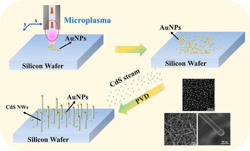
Integrating semiconductor nanowires with silicon platforms can combine the advantages of both materials to provide new functionality compared with each type of material. However, the direct localized growth of semiconductor nanowires on silicon platforms still remains a challenge. Herein, an atmospheric pressure microplasma jet, based on the integration of microplasma with the 3D printing technique, was applied for the synthesis of gold nanoparticles (AuNPs). The obtained AuNPs were then used as catalysts for the physical vapor deposition (PVD) growth of cadmium sulfide nanowires (CdS NWs). The results showed that AuNPs can be directly fabricated on the surface of silicon wafers in one step without chemical reducing agents. They also demonstrated good catalytic activity in the growth of CdS NWs via a typical vapor–liquid–solid (VLS) mechanism, where CdS NWs of straight sidewalls with a AuNP at their tips were formed. Complementary characterization reveals that CdS NWs possess crystalline structure, with the atomic ratio of Cd/S close to 1:1 stoichiometry. The energy band gap was estimated to be 2.5 eV from the photoluminescence spectrum. In addition, the influence of process parameters like the Au3+ concentration and plasma processing time on the products was studied. Both increase of the Au3+ concentration and plasma processing time led to the formation of high-density AuNPs and CdS NWs. With the rise of the Au3+ concentration, the average diameter of the AuNPs gradually increased from 13.17 nm at 0.02 mM to 17.0 nm at 0.05 mM and finally 20.44 nm at 0.1 mM. This also led to the formation of CdS NWs of large diameters. This work offers a simple, direct, and green way for localized fabrication of metal catalysts on target substrates for the growth of NWs and has unprecedented potential in various fields like catalysis, surface modification, and additive manufacturing.
Abstract Image

求助全文
约1分钟内获得全文 求助全文
来源期刊
Industrial & Engineering Chemistry Research
Industrial & Engineering Chemistry Research 工程技术-工程:化工
CiteScore
7.40
自引率
7.10%
发文量
1467
审稿时长
2.8 months
期刊介绍: ndustrial & Engineering Chemistry, with variations in title and format, has been published since 1909 by the American Chemical Society. Industrial & Engineering Chemistry Research is a weekly publication that reports industrial and academic research in the broad fields of applied chemistry and chemical engineering with special focus on fundamentals, processes, and products.
×
引用
GB/T 7714-2015
复制
MLA
复制
APA
复制
导出至
BibTeX EndNote RefMan NoteFirst NoteExpress
×
提示
您的信息不完整,为了账户安全,请先补充。
现在去补充
×
提示
您因"违规操作"
具体请查看互助需知
我知道了
×
提示
确定
请完成安全验证×
copy
已复制链接
快去分享给好友吧!
我知道了
右上角分享
点击右上角分享
0
联系我们:info@booksci.cn Book学术提供免费学术资源搜索服务,方便国内外学者检索中英文文献。致力于提供最便捷和优质的服务体验。 Copyright © 2023 布克学术 All rights reserved.
京ICP备2023020795号-1
ghs 京公网安备 11010802042870号
Book学术文献互助
Book学术文献互助群
群 号:481959085
Book学术官方微信