Physical Vapor Deposition of High-Mobility P-Type Tellurium and Its Applications for Gate-Tunable van der Waals PN Photodiodes

IF 8.3 2区 材料科学 Q1 MATERIALS SCIENCE, MULTIDISCIPLINARY
Tianyi Huang, Sen Lin, Jingyi Zou, Zexiao Wang, Yibai Zhong, Jingwei Li, Ruixuan Wang, Zhixing Wang, Kevin St. Luce, Rex Kim, Jianzhou Cui, Han Wang, Qing Li, Min Xu, Sheng Shen, Xu Zhang
{"title":"Physical Vapor Deposition of High-Mobility P-Type Tellurium and Its Applications for Gate-Tunable van der Waals PN Photodiodes","authors":"Tianyi Huang, Sen Lin, Jingyi Zou, Zexiao Wang, Yibai Zhong, Jingwei Li, Ruixuan Wang, Zhixing Wang, Kevin St. Luce, Rex Kim, Jianzhou Cui, Han Wang, Qing Li, Min Xu, Sheng Shen, Xu Zhang","doi":"10.1021/acsami.4c14865","DOIUrl":null,"url":null,"abstract":"Recently, tellurium has attracted resurgent interest due to its outstanding p-type characteristics and ambient environmental stability. Here, we present a substrate engineering-based physical vapor deposition method to synthesize high-quality Te nanoflakes and achieved a field-effect hole mobility of 1450 cm<sup>2</sup>/(V s), which is, to the best of our knowledge, the highest among existing synthesized two-dimensional p-type semiconductors. The high mobility of Te enables the fabrication of Te/MoS<sub>2</sub> PN diodes with highly gate-tunable characteristics. The Te/MoS<sub>2</sub> heterostructure is demonstrated to be used as visible-light photodetectors with a current responsivity up to 630 A/W, which is about 1 order of magnitude higher than one achieved using p-type Si-MoS<sub>2</sub> PN photodiodes. The photoresponse of Te/MoS<sub>2</sub> heterojunctions also exhibits strong gate tunability due to their ultrathin thickness and unique band alignment. The successful synthesis of high-mobility Te and its integration into Te/MoS<sub>2</sub> photodiodes show promise for the development of highly tunable and multifunctional photodetectors.","PeriodicalId":5,"journal":{"name":"ACS Applied Materials & Interfaces","volume":"72 1","pages":""},"PeriodicalIF":8.3000,"publicationDate":"2024-12-20","publicationTypes":"Journal Article","fieldsOfStudy":null,"isOpenAccess":false,"openAccessPdf":"","citationCount":"0","resultStr":null,"platform":"Semanticscholar","paperid":null,"PeriodicalName":"ACS Applied Materials & Interfaces","FirstCategoryId":"88","ListUrlMain":"https://doi.org/10.1021/acsami.4c14865","RegionNum":2,"RegionCategory":"材料科学","ArticlePicture":[],"TitleCN":null,"AbstractTextCN":null,"PMCID":null,"EPubDate":"","PubModel":"","JCR":"Q1","JCRName":"MATERIALS SCIENCE, MULTIDISCIPLINARY","Score":null,"Total":0}
引用次数: 0

Abstract

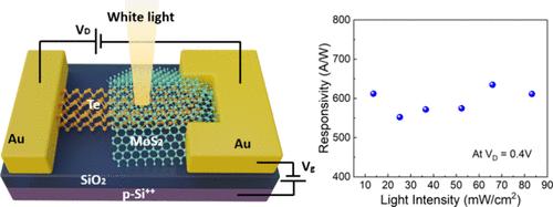
Recently, tellurium has attracted resurgent interest due to its outstanding p-type characteristics and ambient environmental stability. Here, we present a substrate engineering-based physical vapor deposition method to synthesize high-quality Te nanoflakes and achieved a field-effect hole mobility of 1450 cm2/(V s), which is, to the best of our knowledge, the highest among existing synthesized two-dimensional p-type semiconductors. The high mobility of Te enables the fabrication of Te/MoS2 PN diodes with highly gate-tunable characteristics. The Te/MoS2 heterostructure is demonstrated to be used as visible-light photodetectors with a current responsivity up to 630 A/W, which is about 1 order of magnitude higher than one achieved using p-type Si-MoS2 PN photodiodes. The photoresponse of Te/MoS2 heterojunctions also exhibits strong gate tunability due to their ultrathin thickness and unique band alignment. The successful synthesis of high-mobility Te and its integration into Te/MoS2 photodiodes show promise for the development of highly tunable and multifunctional photodetectors.
Abstract Image

高迁移率p型碲的物理气相沉积及其在栅极可调谐范德华PN光电二极管中的应用
最近,碲因其出色的 p 型特性和环境稳定性再次引起了人们的关注。在这里,我们提出了一种基于基底工程的物理气相沉积方法,以合成高质量的纳米碲片,并实现了 1450 cm2/(V s) 的场效应空穴迁移率,据我们所知,这是现有合成的二维 p 型半导体中最高的。Te 的高迁移率使得 Te/MoS2 PN 二极管的制造具有高度的栅极可调特性。实验证明,Te/MoS2 异质结构可用作可见光光电探测器,其电流响应率高达 630 A/W,比使用 p 型 Si-MoS2 PN 光电二极管的电流响应率高出约 1 个数量级。Te/MoS2 异质结的光响应也因其超薄厚度和独特的带排列而表现出很强的栅极可调性。高迁移率碲的成功合成及其与 Te/MoS2 光电二极管的集成,为开发高度可调的多功能光电探测器带来了希望。
本文章由计算机程序翻译,如有差异,请以英文原文为准。
求助全文
约1分钟内获得全文 求助全文
来源期刊
ACS Applied Materials & Interfaces
ACS Applied Materials & Interfaces 工程技术-材料科学:综合
CiteScore
16.00
自引率
6.30%
发文量
4978
审稿时长
1.8 months
期刊介绍: ACS Applied Materials & Interfaces is a leading interdisciplinary journal that brings together chemists, engineers, physicists, and biologists to explore the development and utilization of newly-discovered materials and interfacial processes for specific applications. Our journal has experienced remarkable growth since its establishment in 2009, both in terms of the number of articles published and the impact of the research showcased. We are proud to foster a truly global community, with the majority of published articles originating from outside the United States, reflecting the rapid growth of applied research worldwide.
×
引用
GB/T 7714-2015
复制
MLA
复制
APA
复制
导出至
BibTeX EndNote RefMan NoteFirst NoteExpress
×
提示
您的信息不完整,为了账户安全,请先补充。
现在去补充
×
提示
您因"违规操作"
具体请查看互助需知
我知道了
×
提示
确定
请完成安全验证×
copy
已复制链接
快去分享给好友吧!
我知道了
右上角分享
点击右上角分享
0
联系我们:info@booksci.cn Book学术提供免费学术资源搜索服务,方便国内外学者检索中英文文献。致力于提供最便捷和优质的服务体验。 Copyright © 2023 布克学术 All rights reserved.
京ICP备2023020795号-1
ghs 京公网安备 11010802042870号
Book学术文献互助
Book学术文献互助群
群 号:481959085
Book学术官方微信