Obed Yamín Ramírez-Esquivel, Zeuz Montiel-González, Andrés M. Garay-Tapia, Maria Camila Barrero-Moreno, Francisco Servando Aguirre-Tostado, Dalia Alejandra Mazón-Montijo
{"title":"Mechanisms of Phase Evolution in the Cu–Sb–S System Controlled by the Incorporation of Cu in Sb2S3 Thin Films","authors":"Obed Yamín Ramírez-Esquivel, Zeuz Montiel-González, Andrés M. Garay-Tapia, Maria Camila Barrero-Moreno, Francisco Servando Aguirre-Tostado, Dalia Alejandra Mazón-Montijo","doi":"10.1021/acsami.4c17960","DOIUrl":null,"url":null,"abstract":"Ongoing research in metal chalcogenide semiconductors aims to develop alternative materials for optoelectronic devices. However, due to cost and environmental considerations, there is an increasing emphasis on utilizing green materials. This shift toward sustainable materials and processing is expected to become essential in materials research. In this work, we report the microstructural evolution of thin films of the Cu–Sb–S (CAS) system. The films were obtained by annealing amorphous Sb<sub>2</sub>S<sub>3</sub> precursor films previously immersed in a copper solution with variable residence time. Our main findings demonstrate that varying the residence time in immersion together with the annealing and crystallization of the precursor films leads to a controlled incorporation/distribution of Cu into the films, which promotes the formation of films with phases spanning from a mixture between Sb<sub>2</sub>S<sub>3</sub> and CuSbS<sub>2</sub> to a pure Cu<sub>12</sub>Sb<sub>4</sub>S<sub>13</sub> phase, which represents a significant variation in optoelectronic properties. The phase transition mechanisms were investigated using first-principles calculations and correlated with the structural, morphological, and optoelectronic characterization. Results indicate that vacancies serve as nucleation sites for copper incorporation. Subsequently, interstitial sites are occupied during the phase transformation from Sb<sub>2</sub>S<sub>3</sub> to CuSbS<sub>2</sub>, whereas the transition from CuSbS<sub>2</sub> to Cu<sub>12</sub>Sb<sub>4</sub>S<sub>13</sub> proceeds via a substitutional mechanism. This study contributes to understanding the fundamental phenomena underlying our proposed methodology. These results could promote the development of CAS-based semiconductors with predetermined properties by manipulating simple process parameters, such as the residence time in a copper solution.","PeriodicalId":5,"journal":{"name":"ACS Applied Materials & Interfaces","volume":"146 1","pages":""},"PeriodicalIF":8.3000,"publicationDate":"2024-12-19","publicationTypes":"Journal Article","fieldsOfStudy":null,"isOpenAccess":false,"openAccessPdf":"","citationCount":"0","resultStr":null,"platform":"Semanticscholar","paperid":null,"PeriodicalName":"ACS Applied Materials & Interfaces","FirstCategoryId":"88","ListUrlMain":"https://doi.org/10.1021/acsami.4c17960","RegionNum":2,"RegionCategory":"材料科学","ArticlePicture":[],"TitleCN":null,"AbstractTextCN":null,"PMCID":null,"EPubDate":"","PubModel":"","JCR":"Q1","JCRName":"MATERIALS SCIENCE, MULTIDISCIPLINARY","Score":null,"Total":0}
引用次数: 0
Abstract
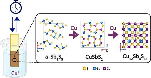
Ongoing research in metal chalcogenide semiconductors aims to develop alternative materials for optoelectronic devices. However, due to cost and environmental considerations, there is an increasing emphasis on utilizing green materials. This shift toward sustainable materials and processing is expected to become essential in materials research. In this work, we report the microstructural evolution of thin films of the Cu–Sb–S (CAS) system. The films were obtained by annealing amorphous Sb2S3 precursor films previously immersed in a copper solution with variable residence time. Our main findings demonstrate that varying the residence time in immersion together with the annealing and crystallization of the precursor films leads to a controlled incorporation/distribution of Cu into the films, which promotes the formation of films with phases spanning from a mixture between Sb2S3 and CuSbS2 to a pure Cu12Sb4S13 phase, which represents a significant variation in optoelectronic properties. The phase transition mechanisms were investigated using first-principles calculations and correlated with the structural, morphological, and optoelectronic characterization. Results indicate that vacancies serve as nucleation sites for copper incorporation. Subsequently, interstitial sites are occupied during the phase transformation from Sb2S3 to CuSbS2, whereas the transition from CuSbS2 to Cu12Sb4S13 proceeds via a substitutional mechanism. This study contributes to understanding the fundamental phenomena underlying our proposed methodology. These results could promote the development of CAS-based semiconductors with predetermined properties by manipulating simple process parameters, such as the residence time in a copper solution.
期刊介绍:
ACS Applied Materials & Interfaces is a leading interdisciplinary journal that brings together chemists, engineers, physicists, and biologists to explore the development and utilization of newly-discovered materials and interfacial processes for specific applications. Our journal has experienced remarkable growth since its establishment in 2009, both in terms of the number of articles published and the impact of the research showcased. We are proud to foster a truly global community, with the majority of published articles originating from outside the United States, reflecting the rapid growth of applied research worldwide.