Equal-Bilayer MoSe2 Grown by a Nucleation-Etching Strategy with High Carrier Mobility
IF 15.8
1区 材料科学
Q1 CHEMISTRY, MULTIDISCIPLINARY
引用次数: 0
Abstract
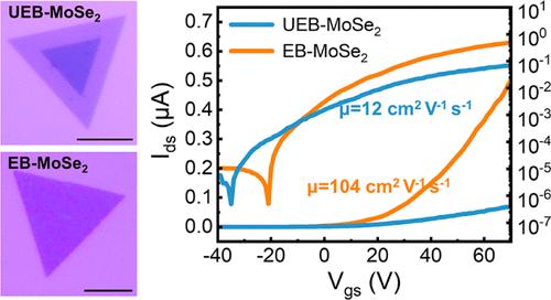
Bilayer transition metal chalcogenides (TMDs) have gradually attracted a great deal of attention due to the higher density of states and carrier mobility than monolayer TMDs. Controlling the uniformity of the layer number is very crucial because it will intensively influence the physical properties. However, it is difficult to synthesize equal-bilayer (EB) TMDs with two identical layers via a normal layer-by-layer strategy. Most reported bilayer TMDs are not uniform and such unequal bilayers would introduce a sizable Schottky barrier, resulting in the low carrier mobility. Here, a nucleation-etching strategy is proposed to grow EB-MoSe2 by chemical vapor deposition (CVD), which breaks the limitations of normal layer-by-layer strategy. The second layer is preferentially formed beneath the first layer rather than above, and a different etching phenomenon is also observed, which occurs more preferentially at the overlapping grain boundary sites on the top layer. The obtained EB-MoSe2 flakes are 3R-stack with high crystal quality. Furthermore, the contact between EB-MoSe2 and metal electrodes is greatly improved, thereby EB-MoSe2 transistors exhibit an order of magnitude higher carrier mobility (104 cm2 V–1 s–1) than that of UEB-MoSe2 transistors (12 cm2 V–1 s–1). This value is also at a relatively high level compared with reported results. Our work offers a feasible strategy for the synthesis of EB-TMDs with high carrier mobility, which is meaningful for developing high-performance 2D optoelectronic devices.
高载流子迁移率的等双层MoSe2成核蚀刻生长方法
双层过渡金属硫族化合物由于具有比单层过渡金属硫族化合物更高的态密度和载流子迁移率而逐渐引起人们的广泛关注。层数的均匀性对材料的物理性能影响很大,因此控制层数的均匀性至关重要。然而,通过常规的逐层策略很难合成具有两个相同层的等双层(EB) tmd。大多数报道的双层tmd是不均匀的,这种不均匀的双层会引入相当大的肖特基势垒,导致载流子迁移率低。本文提出了一种化学气相沉积(CVD)生长EB-MoSe2的成核蚀刻策略,突破了常规逐层生长策略的局限性。第二层优先形成于第一层的下方而不是上方,并且还观察到一种不同的蚀刻现象,这种现象更优先发生在顶层重叠的晶界位置。所得EB-MoSe2薄片为3r堆叠,晶体质量高。此外,EB-MoSe2与金属电极之间的接触大大改善,因此EB-MoSe2晶体管的载流子迁移率(104 cm2 V-1 s-1)比UEB-MoSe2晶体管(12 cm2 V-1 s-1)高了一个数量级。与报告的结果相比,该值也处于相对较高的水平。我们的工作为合成具有高载流子迁移率的eb - tmd提供了一种可行的策略,这对开发高性能的二维光电器件具有重要意义。
本文章由计算机程序翻译,如有差异,请以英文原文为准。
求助全文
约1分钟内获得全文
求助全文
来源期刊

ACS Nano
工程技术-材料科学:综合
CiteScore
26.00
自引率
4.10%
发文量
1627
审稿时长
1.7 months
期刊介绍:
ACS Nano, published monthly, serves as an international forum for comprehensive articles on nanoscience and nanotechnology research at the intersections of chemistry, biology, materials science, physics, and engineering. The journal fosters communication among scientists in these communities, facilitating collaboration, new research opportunities, and advancements through discoveries. ACS Nano covers synthesis, assembly, characterization, theory, and simulation of nanostructures, nanobiotechnology, nanofabrication, methods and tools for nanoscience and nanotechnology, and self- and directed-assembly. Alongside original research articles, it offers thorough reviews, perspectives on cutting-edge research, and discussions envisioning the future of nanoscience and nanotechnology.
文献相关原料
公司名称
产品信息
阿拉丁
Molybdenum trioxide (MoO3)
阿拉丁
Molybdenum trioxide (MoO3)
 求助内容:
求助内容: 应助结果提醒方式:


