Fast and Efficient Sub-Band Gap Photodetection in Al:ZnO/Si Heterojunction by Enhanced Photoexcited Hole Transport via Interfacial Defect States

IF 6.5 1区 物理与天体物理 Q1 MATERIALS SCIENCE, MULTIDISCIPLINARY
Geunpil Kim, Byung Chul Lee, Jongbum Kim
{"title":"Fast and Efficient Sub-Band Gap Photodetection in Al:ZnO/Si Heterojunction by Enhanced Photoexcited Hole Transport via Interfacial Defect States","authors":"Geunpil Kim, Byung Chul Lee, Jongbum Kim","doi":"10.1021/acsphotonics.4c01057","DOIUrl":null,"url":null,"abstract":"This study focuses on sub-band gap photodetection in n<sup>+</sup>-Al:ZnO/n-Si isotype heterojunction-based photodiodes via interfacial defects induced by metal oxide films. Through comparative studies on the photoresponse of Schottky junction-based photodiodes with the modified electronic band structure by controlling the structural and electrical properties of Al:ZnO films, as well as the Si substrate’s doping level, we investigate the underlying mechanisms of interfacial defect states for sub-band gap photodetection in Si. Our analysis suggests that these interfacial defects not only act as additional sources for photoexcited carrier generations but also serve as pathways for photogenerated holes in the Si valence band, enabling their flow into the Al:ZnO film and improving the operating speed. Time-resolved photocurrent measurements under near-infrared illumination illustrate an enhancement in photocurrent with lower oxygen partial pressures (0 mTorr) attributed to alterations in the energy band structure caused by interfacial defect states. Significantly, the Al:ZnO/Si photodiode fabricated under optimized conditions exhibits a photoresponse of 2.48 mA/W at 1310 nm with fast rise/fall times of 5.5/5.25 μs at 1 kHz and a 3 dB bandwidth of approximately 150 kHz, without introducing additional bulk trap states in Si. In light of these findings, the combination of simple fabrication and excellent switching speed of interfacial defect-mediated Si photodiodes has the potential to significantly impact the technologies of Si photonics and advanced Si-based photoelectric devices.","PeriodicalId":23,"journal":{"name":"ACS Photonics","volume":"48 1","pages":""},"PeriodicalIF":6.5000,"publicationDate":"2024-12-18","publicationTypes":"Journal Article","fieldsOfStudy":null,"isOpenAccess":false,"openAccessPdf":"","citationCount":"0","resultStr":null,"platform":"Semanticscholar","paperid":null,"PeriodicalName":"ACS Photonics","FirstCategoryId":"101","ListUrlMain":"https://doi.org/10.1021/acsphotonics.4c01057","RegionNum":1,"RegionCategory":"物理与天体物理","ArticlePicture":[],"TitleCN":null,"AbstractTextCN":null,"PMCID":null,"EPubDate":"","PubModel":"","JCR":"Q1","JCRName":"MATERIALS SCIENCE, MULTIDISCIPLINARY","Score":null,"Total":0}
引用次数: 0

Abstract

This study focuses on sub-band gap photodetection in n+-Al:ZnO/n-Si isotype heterojunction-based photodiodes via interfacial defects induced by metal oxide films. Through comparative studies on the photoresponse of Schottky junction-based photodiodes with the modified electronic band structure by controlling the structural and electrical properties of Al:ZnO films, as well as the Si substrate’s doping level, we investigate the underlying mechanisms of interfacial defect states for sub-band gap photodetection in Si. Our analysis suggests that these interfacial defects not only act as additional sources for photoexcited carrier generations but also serve as pathways for photogenerated holes in the Si valence band, enabling their flow into the Al:ZnO film and improving the operating speed. Time-resolved photocurrent measurements under near-infrared illumination illustrate an enhancement in photocurrent with lower oxygen partial pressures (0 mTorr) attributed to alterations in the energy band structure caused by interfacial defect states. Significantly, the Al:ZnO/Si photodiode fabricated under optimized conditions exhibits a photoresponse of 2.48 mA/W at 1310 nm with fast rise/fall times of 5.5/5.25 μs at 1 kHz and a 3 dB bandwidth of approximately 150 kHz, without introducing additional bulk trap states in Si. In light of these findings, the combination of simple fabrication and excellent switching speed of interfacial defect-mediated Si photodiodes has the potential to significantly impact the technologies of Si photonics and advanced Si-based photoelectric devices.
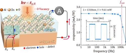
Abstract Image

基于界面缺陷态增强光激发空穴输运的Al:ZnO/Si异质结快速高效亚带隙光检测
本文主要研究了利用金属氧化物薄膜引起的界面缺陷对n+-Al:ZnO/n- si异质结型光电二极管进行亚带隙光探测。通过对比研究通过控制Al:ZnO薄膜的结构和电学性质以及Si衬底的掺杂水平来修饰电子带结构的肖特基结光电二极管的光响应,我们探讨了Si中亚带隙光探测界面缺陷状态的潜在机制。我们的分析表明,这些界面缺陷不仅作为光激发载流子生成的额外来源,而且还作为Si价带中光生成空穴的途径,使它们能够流入Al:ZnO薄膜并提高运行速度。近红外照明下的时间分辨光电流测量表明,由于界面缺陷态引起的能带结构改变,当氧分压(0 mTorr)较低时,光电流增强。值得注意的是,在优化条件下制备的Al:ZnO/Si光电二极管在1310 nm处的光响应为2.48 mA/W,在1 kHz时的快速上升/下降时间为5.5/5.25 μs,带宽约为150 kHz,而无需在Si中引入额外的体阱态。鉴于这些发现,界面缺陷介导的硅光电二极管的简单制造和优异的开关速度相结合,有可能显著影响硅光子学技术和先进的硅基光电器件。
本文章由计算机程序翻译,如有差异,请以英文原文为准。
求助全文
约1分钟内获得全文 求助全文
来源期刊
ACS Photonics
ACS Photonics NANOSCIENCE & NANOTECHNOLOGY-MATERIALS SCIENCE, MULTIDISCIPLINARY
CiteScore
11.90
自引率
5.70%
发文量
438
审稿时长
2.3 months
期刊介绍: Published as soon as accepted and summarized in monthly issues, ACS Photonics will publish Research Articles, Letters, Perspectives, and Reviews, to encompass the full scope of published research in this field.
×
引用
GB/T 7714-2015
复制
MLA
复制
APA
复制
导出至
BibTeX EndNote RefMan NoteFirst NoteExpress
×
提示
您的信息不完整,为了账户安全,请先补充。
现在去补充
×
提示
您因"违规操作"
具体请查看互助需知
我知道了
×
提示
确定
请完成安全验证×
copy
已复制链接
快去分享给好友吧!
我知道了
右上角分享
点击右上角分享
0
联系我们:info@booksci.cn Book学术提供免费学术资源搜索服务,方便国内外学者检索中英文文献。致力于提供最便捷和优质的服务体验。 Copyright © 2023 布克学术 All rights reserved.
京ICP备2023020795号-1
ghs 京公网安备 11010802042870号
Book学术文献互助
Book学术文献互助群
群 号:481959085
Book学术官方微信