Electron-Beam-Induced Negative Differential Transconductance Homojunction Device Based on van der Waals Materials for Functionally Complete Ternary Computing
IF 15.8
1区 材料科学
Q1 CHEMISTRY, MULTIDISCIPLINARY
引用次数: 0
Abstract
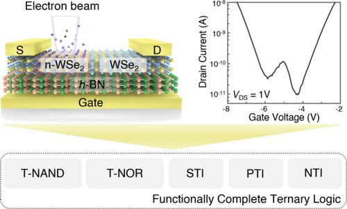
Negative differential transconductance (NDT) devices have emerged as promising candidates for multivalued logic computing, and particularly for ternary logic systems. To enable computation of any ternary operation, it is essential to have a functionally complete set of ternary logic gates, which remains unrealized with current NDT technologies, posing a critical limitation for higher-level circuit design. Additionally, NDT devices typically rely on heterojunctions, complicating fabrication and impacting reliability due to the introduction of additional materials and interfaces. Here, we utilize an electron beam to develop tungsten diselenide (WSe2) homojunction NDT devices with W-shaped current–voltage (I–V) characteristics. We demonstrate that electron beam enables the manipulation of Se atoms in WSe2, facilitating controllable and spatially precise tailoring of the WSe2 work function. The electron-beam treatment applied to a part of the WSe2 channel induces a lateral homojunction and ultimately results in the W-shaped I–V curves, which enable both one-input and two-input ternary logic gates. We propose and implement a balanced circuit design for two-input ternary NAND, AND, NOR, and OR gates, featuring a low device count, full-swing operation, and minimized output signal variations. Together with three types of ternary inverters also designed in this work, they form a functionally complete set of ternary logic gates─a prerequisite for practical ternary computing. This work addresses a critical gap in the development of NDT-based ternary computing by ensuring functional completeness and highlights the versatility of electron-beam treatment as an engineering tool for tailoring the properties of two-dimensional van der Waals materials.

基于范德华材料的电子束诱导负差分跨导同结器件的功能完全三元计算
负差分跨导(NDT)器件已成为多值逻辑计算,特别是三元逻辑系统的有前途的候选者。为了实现任何三元运算的计算,必须有一套功能完整的三元逻辑门,这在当前的无损检测技术中仍然无法实现,这对更高级别的电路设计构成了严重的限制。此外,无损检测设备通常依赖于异质结,由于引入了额外的材料和界面,使得制造复杂化并影响可靠性。在这里,我们利用电子束来开发具有w形电流-电压(I-V)特性的二硒化钨(WSe2)同质结无损检测器件。我们证明了电子束能够操纵WSe2中的Se原子,促进了WSe2功函数的可控和空间精确剪裁。电子束处理部分WSe2通道诱导了横向同质结,最终形成了w形的I-V曲线,从而实现了单输入和双输入三元逻辑门。我们提出并实现了一种用于双输入三元NAND, and, NOR和OR门的平衡电路设计,具有低器件计数,全摆幅操作和最小输出信号变化的特点。与本研究中设计的三种类型的三元逆变器一起,它们形成了一套功能完整的三元逻辑门──这是实际三元计算的先决条件。这项工作通过确保功能完整性解决了基于ndt的三元计算发展中的一个关键空白,并强调了电子束处理作为定制二维范德华材料特性的工程工具的多功能性。
本文章由计算机程序翻译,如有差异,请以英文原文为准。
求助全文
约1分钟内获得全文
求助全文
来源期刊

ACS Nano
工程技术-材料科学:综合
CiteScore
26.00
自引率
4.10%
发文量
1627
审稿时长
1.7 months
期刊介绍:
ACS Nano, published monthly, serves as an international forum for comprehensive articles on nanoscience and nanotechnology research at the intersections of chemistry, biology, materials science, physics, and engineering. The journal fosters communication among scientists in these communities, facilitating collaboration, new research opportunities, and advancements through discoveries. ACS Nano covers synthesis, assembly, characterization, theory, and simulation of nanostructures, nanobiotechnology, nanofabrication, methods and tools for nanoscience and nanotechnology, and self- and directed-assembly. Alongside original research articles, it offers thorough reviews, perspectives on cutting-edge research, and discussions envisioning the future of nanoscience and nanotechnology.
 求助内容:
求助内容: 应助结果提醒方式:


