Nickel films deposited between amorphous silicon layers: Effects of annealing, Ni/Si interface and magnetic properties
IF 6.9
2区 材料科学
Q2 CHEMISTRY, PHYSICAL
引用次数: 0
Abstract
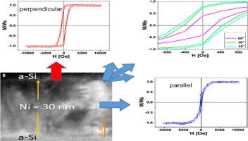
This study demonstrates exceptional magnetic properties associated with magnetic anisotropy in nickel layers approximately 23–28 nm thick, deposited between amorphous silicon layers (a-Si/Ni/a-Si) using triode sputtering. X-ray diffraction (XRD) analyses confirm the presence of the Ni phase in the samples. Furthermore, transmission electron microscopy (TEM) and X-ray photoelectron spectroscopy (XPS) measurements reveal a trilayer structure consisting of nickel and silicon. These techniques also highlight the surface roughness of the nickel layer and detail the characteristics of the Ni/Si interface. Magnetic properties were evaluated using a vibrating sample magnetometer (VSM). The samples were annealed at temperatures up to 190 °C to optimize their magnetic characteristics. After annealing, the samples exhibited a high perpendicular remanence ratio (Mr/MS ≈ 1), high perpendicular coercivity (HC = 620 Oe), and a high effective perpendicular magnetic anisotropy energy density (Keff*t ≈ 1.16 erg/cm2). These properties are particularly interesting because of the substantial thickness of the nickel layer. Achieving nickel films thicker than 15 nm with perpendicular magnetic anisotropy (PMA) has been challenging. The origin of PMA is attributed to magnetoelastic anisotropy and internal strains, which are related to diffusion processes and thermal expansion mismatch between the Ni layer and the Ni/Si and a-Si layers.

非晶硅层间镍膜的沉积:退火、Ni/Si界面及磁性能的影响
该研究证明了在非晶硅层(a-Si/Ni/a-Si)之间使用三极管溅射沉积的约23-28 nm厚的镍层中,与磁性各向异性相关的特殊磁性。x射线衍射(XRD)分析证实了样品中镍相的存在。此外,透射电子显微镜(TEM)和x射线光电子能谱(XPS)测量显示镍和硅组成的三层结构。这些技术还突出了镍层的表面粗糙度,并详细描述了Ni/Si界面的特征。用振动样品磁强计(VSM)评价其磁性能。样品在高达190 °C的温度下退火,以优化其磁性。退火后,样品具有较高的垂直剩磁比(Mr/MS≈1)、较高的垂直矫顽力(HC = 620 Oe)和较高的有效垂直磁各向异性能密度(Keff*t≈1.16 erg/cm2)。由于镍层的厚度很大,这些特性特别有趣。获得厚度大于15 nm且具有垂直磁各向异性(PMA)的镍膜一直是一个挑战。PMA的成因是磁弹性各向异性和内部应变,这与Ni层与Ni/Si和a-Si层之间的扩散过程和热膨胀失配有关。
本文章由计算机程序翻译,如有差异,请以英文原文为准。
求助全文
约1分钟内获得全文
求助全文
来源期刊

Applied Surface Science
工程技术-材料科学:膜
CiteScore
12.50
自引率
7.50%
发文量
3393
审稿时长
67 days
期刊介绍:
Applied Surface Science covers topics contributing to a better understanding of surfaces, interfaces, nanostructures and their applications. The journal is concerned with scientific research on the atomic and molecular level of material properties determined with specific surface analytical techniques and/or computational methods, as well as the processing of such structures.
 求助内容:
求助内容: 应助结果提醒方式:


