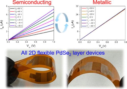
Introducing Semiconducting-to-Metallic Transitions into Wafer-Scale 2D PdSe2 Layers by Low-Temperature Anion Exchange and Thickness Modulation
IF 15.8
1区 材料科学
Q1 CHEMISTRY, MULTIDISCIPLINARY
引用次数: 0
Abstract
Two-dimensional (2D) palladium diselenide (PdSe2) layers are projected to exhibit a number of intriguing electrical properties such as semiconducting-to-metallic transitions. Precisely modulating their morphology and chemistry is essential for realizing such opportunities, which is particularly demanded on a large dimension under flexible processing conditions toward broadening their practical device applicability. Herein, we explore a wafer-scale growth of 2D PdSe2 layers and introduce semiconducting-to-metallic transitions into them at as low as 330 °C, a temperature compatible with a range of polymeric substrates as well as the back-end-of-line (BEOL) processes. Two independent physical and chemical approaches of thickness modulation and anion exchange are demonstrated to induce the low-temperature-driven electrical transitions. Wafer-scale 2D PdSe2 layers grown from a scalable selenization of thin (∼2 nm) Pd exhibit p-type semiconducting characteristics, which completely vanish with increasing thickness. Furthermore, a postgrowth reaction involving an exchange of selenium (Se)-to-tellurium (Te) ions chemically introduces the semiconducting-to-metallic transitions through the conversion of PdSe2-to-palladium ditelluride (PdTe2). A significant reduction of the bandgap energy from 0.7 to 0 V is observed to be associated with the transitions, while the converted 2D layers remain to be highly metallic irrespective of thickness variations. These controlled transition characteristics are employed to fabricate “all-2D” flexible devices employing semiconducting 2D layer channels and metallic 2D layer electrodes on a wafer-scale.

通过低温阴离子交换和厚度调制在晶圆级二维钯硒层中引入半导体到金属的转变
二维(2D)二硒化钯(PdSe2)层预计将表现出许多有趣的电学性质,如半导体到金属的转变。精确地调制它们的形态和化学对于实现这些机会至关重要,这在灵活的加工条件下特别需要在大尺寸上扩大它们的实际设备适用性。在此,我们探索了二维PdSe2层的晶圆级生长,并在低至330°C的温度下引入半导体到金属的转变,该温度与一系列聚合物衬底以及后端线(BEOL)工艺兼容。通过厚度调制和阴离子交换两种独立的物理和化学方法来诱导低温驱动的电跃迁。从可扩展硒化薄(~ 2 nm) Pd生长的晶圆级2D PdSe2层表现出p型半导体特性,随着厚度的增加完全消失。此外,生长后反应涉及硒(Se)到碲(Te)离子的交换,通过pdse2到二碲化钯(PdTe2)的转化,化学上引入了半导体到金属的转变。观察到带隙能量从0.7 V显著降低到0 V与转换有关,而转换后的二维层无论厚度变化如何都保持高度金属化。利用这些受控的过渡特性,在晶圆尺度上采用半导体2D层通道和金属2D层电极制造“全2D”柔性器件。
本文章由计算机程序翻译,如有差异,请以英文原文为准。
求助全文
约1分钟内获得全文
求助全文
来源期刊

ACS Nano
工程技术-材料科学:综合
CiteScore
26.00
自引率
4.10%
发文量
1627
审稿时长
1.7 months
期刊介绍:
ACS Nano, published monthly, serves as an international forum for comprehensive articles on nanoscience and nanotechnology research at the intersections of chemistry, biology, materials science, physics, and engineering. The journal fosters communication among scientists in these communities, facilitating collaboration, new research opportunities, and advancements through discoveries. ACS Nano covers synthesis, assembly, characterization, theory, and simulation of nanostructures, nanobiotechnology, nanofabrication, methods and tools for nanoscience and nanotechnology, and self- and directed-assembly. Alongside original research articles, it offers thorough reviews, perspectives on cutting-edge research, and discussions envisioning the future of nanoscience and nanotechnology.
 求助内容:
求助内容: 应助结果提醒方式:


