Ultrawide Bandgap Diamond/ε-Ga2O3 Heterojunction pn Diodes with Breakdown Voltages over 3 kV
IF 9.1
1区 材料科学
Q1 CHEMISTRY, MULTIDISCIPLINARY
引用次数: 0
Abstract
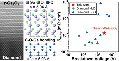
Robust bipolar devices based on exclusively ultrawide bandgap (UWBG) semiconductors are highly desired for advanced power electronics. The heterojunction strategy has been a prevailing method for fabricating a bipolar device due to the lack of effective bipolar doping in the same UWBG material. Here, we demonstrate a unique heterojunction design integrating the p-type diamond and n-type ε-Ga2O3 that achieves remarkable breakdown voltages surpassing 3000 V. Despite the lattice mismatch, the heteroepitaxial ε-Ga2O3 film is established on the diamond substrate, forming an atomically sharp interface with C–O–Ga bonding and enabling the O-terminated diamond surface for constructing an effective rectifying heterojunction. The ultra-high-quality interface, together with the lightly doped diamond as the drift layer, largely weakens the commonly met electric field crowding effect in power diodes and provides a cost-effective thermal management route. This study provides an efficient heterojunction design to realize the potential of UWBG semiconductors for ultra-high-power applications.
击穿电压超过 3 kV 的超宽带隙金刚石/ε-Ga2O3 异质结 pn 二极管
基于超宽带隙(UWBG)半导体的稳健双极器件是先进电力电子器件的迫切需求。由于在同一UWBG材料中缺乏有效的双极掺杂,异质结策略一直是制造双极器件的主流方法。在这里,我们展示了一种独特的异质结设计,将p型金刚石和n型ε-Ga2O3集成在一起,实现了超过3000 V的显著击穿电压。尽管晶格不匹配,但在金刚石衬底上建立了异质外延ε-Ga2O3薄膜,形成了与C-O-Ga键合的原子锋利界面,使o端金刚石表面能够构建有效的整流异质结。超高质量的界面加上轻掺杂的金刚石作为漂移层,大大削弱了功率二极管中常见的电场拥挤效应,提供了一种经济有效的热管理途径。该研究提供了一种高效的异质结设计,以实现UWBG半导体在超高功率应用中的潜力。
本文章由计算机程序翻译,如有差异,请以英文原文为准。
求助全文
约1分钟内获得全文
求助全文
来源期刊

Nano Letters
工程技术-材料科学:综合
CiteScore
16.80
自引率
2.80%
发文量
1182
审稿时长
1.4 months
期刊介绍:
Nano Letters serves as a dynamic platform for promptly disseminating original results in fundamental, applied, and emerging research across all facets of nanoscience and nanotechnology. A pivotal criterion for inclusion within Nano Letters is the convergence of at least two different areas or disciplines, ensuring a rich interdisciplinary scope. The journal is dedicated to fostering exploration in diverse areas, including:
- Experimental and theoretical findings on physical, chemical, and biological phenomena at the nanoscale
- Synthesis, characterization, and processing of organic, inorganic, polymer, and hybrid nanomaterials through physical, chemical, and biological methodologies
- Modeling and simulation of synthetic, assembly, and interaction processes
- Realization of integrated nanostructures and nano-engineered devices exhibiting advanced performance
- Applications of nanoscale materials in living and environmental systems
Nano Letters is committed to advancing and showcasing groundbreaking research that intersects various domains, fostering innovation and collaboration in the ever-evolving field of nanoscience and nanotechnology.
 求助内容:
求助内容: 应助结果提醒方式:


