Three-dimensional transistors with two-dimensional semiconductors for future CMOS scaling
IF 33.7
1区 工程技术
Q1 ENGINEERING, ELECTRICAL & ELECTRONIC
引用次数: 0
Abstract
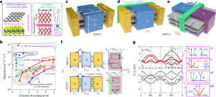
Atomically thin two-dimensional (2D) semiconductors—particularly transition metal dichalcogenides—are potential channel materials for post-silicon complementary metal–oxide–semiconductor (CMOS) field-effect transistors. However, their application in CMOS technology will require implementation in three-dimensional (3D) transistors. Here we report a framework for designing scaled 3D transistors using 2D semiconductors. Our approach is based on non-equilibrium Green’s function quantum transport simulations that incorporate the effects of non-ideal Schottky contacts and inclusive capacitance calculations, with material inputs derived from density functional theory simulations. A comparative performance analysis of different 3D transistors (2D and silicon based) and channel thicknesses is carried out for both low-standby-power and high-performance applications. This suggests that trilayer tungsten disulfide is the most promising material, offering an improvement in energy–delay product of over 55% compared with silicon counterparts, potentially extending CMOS scaling down to a few nanometres. We also show that 2D semiconductors could be uniquely engineered to create 2D nanoplate field-effect transistors that offer nearly tenfold improvement in integration density and drive current over both 2D- and silicon-based 3D field-effect transistors with similar footprints. A simulation framework for three-dimensionally structured transistors based on two-dimensional materials shows that they could be used to continue complementary metal–oxide–semiconductor scaling with performance and energy enhancements.


三维晶体管与二维半导体的未来CMOS缩放
原子薄的二维(2D)半导体,特别是过渡金属二掺杂物,是硅后互补金属氧化物半导体(CMOS)场效应晶体管的潜在沟道材料。然而,它们在 CMOS 技术中的应用需要在三维(3D)晶体管中实现。在此,我们报告了一个利用二维半导体设计缩放三维晶体管的框架。我们的方法基于非平衡格林函数量子传输模拟,其中包含了非理想肖特基触点和包容性电容计算的影响,以及从密度泛函理论模拟中获得的材料输入。针对低待机功率和高性能应用,对不同三维晶体管(二维和硅基)和沟道厚度进行了性能比较分析。结果表明,三层二硫化钨是最有前途的材料,与硅材料相比,其能延积提高了 55% 以上,有可能将 CMOS 扩展到几纳米。我们还表明,可以对二维半导体进行独特的工程设计,制造出二维纳米板场效应晶体管,与具有类似基底面的二维和硅基三维场效应晶体管相比,这种晶体管的集成密度和驱动电流提高了近十倍。
本文章由计算机程序翻译,如有差异,请以英文原文为准。
求助全文
约1分钟内获得全文
求助全文
来源期刊

Nature Electronics
Engineering-Electrical and Electronic Engineering
CiteScore
47.50
自引率
2.30%
发文量
159
期刊介绍:
Nature Electronics is a comprehensive journal that publishes both fundamental and applied research in the field of electronics. It encompasses a wide range of topics, including the study of new phenomena and devices, the design and construction of electronic circuits, and the practical applications of electronics. In addition, the journal explores the commercial and industrial aspects of electronics research.
The primary focus of Nature Electronics is on the development of technology and its potential impact on society. The journal incorporates the contributions of scientists, engineers, and industry professionals, offering a platform for their research findings. Moreover, Nature Electronics provides insightful commentary, thorough reviews, and analysis of the key issues that shape the field, as well as the technologies that are reshaping society.
Like all journals within the prestigious Nature brand, Nature Electronics upholds the highest standards of quality. It maintains a dedicated team of professional editors and follows a fair and rigorous peer-review process. The journal also ensures impeccable copy-editing and production, enabling swift publication. Additionally, Nature Electronics prides itself on its editorial independence, ensuring unbiased and impartial reporting.
In summary, Nature Electronics is a leading journal that publishes cutting-edge research in electronics. With its multidisciplinary approach and commitment to excellence, the journal serves as a valuable resource for scientists, engineers, and industry professionals seeking to stay at the forefront of advancements in the field.
 求助内容:
求助内容: 应助结果提醒方式:


