The current–voltage (I–V) characteristics and low–high impedance measurements (C/G–V) of Au/(AgCdS:PVP)/n-Si Schottky diode (SD) at dark and under illumination conditions
IF 2.8 4区 工程技术Q2 ENGINEERING, ELECTRICAL & ELECTRONIC
G. Aslanbaş, P. Durmuş, Ş. Altındal, Y. Azizian-Kalandaragh
{"title":"The current–voltage (I–V) characteristics and low–high impedance measurements (C/G–V) of Au/(AgCdS:PVP)/n-Si Schottky diode (SD) at dark and under illumination conditions","authors":"G. Aslanbaş, P. Durmuş, Ş. Altındal, Y. Azizian-Kalandaragh","doi":"10.1007/s10854-024-14014-0","DOIUrl":null,"url":null,"abstract":"<div><p>In this study, Schottky diode (SD) with a structure of Au/(AgCdS:PVP)/n-Si has been fabricated and then its electrical parameters and conduction mechanisms (CMs) investigated by measuring current–voltage (I–V) and capacitance/conductance–voltage (C/G–V) data in dark and under 100-mW cm<sup>−2</sup> illumination intensity at room temperature (RT). These measurements show that almost all basic electrical parameters and CM depend on illumination, frequency, and voltage. The energy/voltage-dependent profile of surface states (<i>N</i><sub>ss</sub>) was extracted from the forward bias I–V data considering voltage dependence of ideality factor (<i>n</i>), barrier height, and low/high-frequency capacitance model. The density of doping atoms (<i>N</i><sub>d</sub>), barrier height (Φ<sub>B</sub>(C–V)), and the width of depletion region (<i>W</i><sub>d</sub>) were also computed by the linear zone of the reverse bias C<sup>−2</sup>–V plot at a frequency of 1 MHz, and the dark conditions. The maximum photosensitivity and photoresponsivity were found as 384 and 7.5 mW A<sup>−1</sup> under 100 mW cm<sup>−2</sup>, respectively. Based on the experimental findings, the Au/(AgCdS:PVP)/n-Si SD has good rectifier and photodiode behavior and hence, it can be successfully used in electronic and optoelectronic applications rather than conventional metal–semiconductor (MS)-type SD with/without an insulator layer grown by traditional techniques considering the advantages of polymers, such as high mechanical strength, low-cost production, and low energy consumption.</p></div>","PeriodicalId":646,"journal":{"name":"Journal of Materials Science: Materials in Electronics","volume":"35 36","pages":""},"PeriodicalIF":2.8000,"publicationDate":"2024-12-14","publicationTypes":"Journal Article","fieldsOfStudy":null,"isOpenAccess":false,"openAccessPdf":"","citationCount":"0","resultStr":null,"platform":"Semanticscholar","paperid":null,"PeriodicalName":"Journal of Materials Science: Materials in Electronics","FirstCategoryId":"5","ListUrlMain":"https://link.springer.com/article/10.1007/s10854-024-14014-0","RegionNum":4,"RegionCategory":"工程技术","ArticlePicture":[],"TitleCN":null,"AbstractTextCN":null,"PMCID":null,"EPubDate":"","PubModel":"","JCR":"Q2","JCRName":"ENGINEERING, ELECTRICAL & ELECTRONIC","Score":null,"Total":0}
引用次数: 0
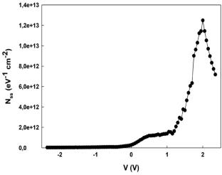
Abstract
In this study, Schottky diode (SD) with a structure of Au/(AgCdS:PVP)/n-Si has been fabricated and then its electrical parameters and conduction mechanisms (CMs) investigated by measuring current–voltage (I–V) and capacitance/conductance–voltage (C/G–V) data in dark and under 100-mW cm−2 illumination intensity at room temperature (RT). These measurements show that almost all basic electrical parameters and CM depend on illumination, frequency, and voltage. The energy/voltage-dependent profile of surface states (Nss) was extracted from the forward bias I–V data considering voltage dependence of ideality factor (n), barrier height, and low/high-frequency capacitance model. The density of doping atoms (Nd), barrier height (ΦB(C–V)), and the width of depletion region (Wd) were also computed by the linear zone of the reverse bias C−2–V plot at a frequency of 1 MHz, and the dark conditions. The maximum photosensitivity and photoresponsivity were found as 384 and 7.5 mW A−1 under 100 mW cm−2, respectively. Based on the experimental findings, the Au/(AgCdS:PVP)/n-Si SD has good rectifier and photodiode behavior and hence, it can be successfully used in electronic and optoelectronic applications rather than conventional metal–semiconductor (MS)-type SD with/without an insulator layer grown by traditional techniques considering the advantages of polymers, such as high mechanical strength, low-cost production, and low energy consumption.
期刊介绍:
The Journal of Materials Science: Materials in Electronics is an established refereed companion to the Journal of Materials Science. It publishes papers on materials and their applications in modern electronics, covering the ground between fundamental science, such as semiconductor physics, and work concerned specifically with applications. It explores the growth and preparation of new materials, as well as their processing, fabrication, bonding and encapsulation, together with the reliability, failure analysis, quality assurance and characterization related to the whole range of applications in electronics. The Journal presents papers in newly developing fields such as low dimensional structures and devices, optoelectronics including III-V compounds, glasses and linear/non-linear crystal materials and lasers, high Tc superconductors, conducting polymers, thick film materials and new contact technologies, as well as the established electronics device and circuit materials.

 求助内容:
求助内容: 应助结果提醒方式:


