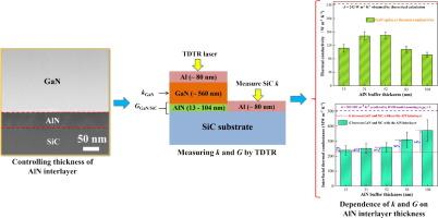
Effect of AlN interlayer thickness on thermal conductances of GaN epilayer and GaN/SiC interface in GaN-on-SiC heterostructures
IF 6.3
2区 材料科学
Q2 CHEMISTRY, PHYSICAL
引用次数: 0
Abstract
The temperature rise in GaN-on-SiC based high electron mobility transistors (HEMTs) is firmly dependent on the thermal conductivity (k) of GaN epilayer and the interfacial thermal conductance (G) between GaN and SiC. The AlN buffer is usually utilized during the heteroepitaxial growth of GaN on SiC substrate, while the effects of its thickness on k and G are still not clear. In this study, the GaN/AlN/SiC multilayer structure is prepared by metal–organic chemical vapor deposition, and aiding by time-domain thermoreflectance, we detect how the thickness of AlN interlayer influences k and G. The results reveal that the AlN interlayer evolves from serrated island shape to smooth planar form with increasing its thickness from 13 to 104 nm, which induces that the tensile stress of the subsequently grown GaN firstly decreases and then increases, giving a minimum value of 339 MPa at 52 nm-thick AlN. Consequently, a maximal k of 150 W m−1 K−1 for the GaN epilayer is achieved. Moreover, the AlN interlayer is beneficial to the enhancement of G due to the improved overlap of phonon density of states, and an increase of G by up to 64% can be realized via an insertion of 104 nm-thick AlN, which could be the consequence of both atomically smooth interfaces and the improved crystal quality of thicker AlN. The findings clearly manifest the effect of AlN interlayer thickness on the k and G of GaN/AlN/SiC structures, which provides guidelines for preparation of multilayer structures helping to minimize the thermal resistance of HEMTs.


氮化镓层间厚度对氮化镓-碳化硅异质结构中氮化镓外延层和氮化镓/碳化硅界面热导的影响
基于碳化硅基氮化镓的高电子迁移率晶体管(HEMT)的温升与氮化镓外延层的热导率(k)以及氮化镓和碳化硅之间的界面热导率(G)密切相关。氮化镓在碳化硅衬底上进行异质外延生长时通常会使用氮化镓缓冲层,但其厚度对 k 和 G 的影响尚不清楚。本研究采用金属有机化学气相沉积法制备了 GaN/AlN/SiC 多层结构,并借助时域热反射法检测了 AlN 夹层厚度对 k 和 G 的影响。结果表明,随着 AlN 中间膜厚度从 13 纳米增加到 104 纳米,其形状从锯齿岛状演变为光滑的平面状,这导致随后生长的 GaN 的拉伸应力先减小后增大,在 52 纳米厚的 AlN 上,拉伸应力的最小值为 339 兆帕。因此,氮化镓外延层的最大 k 值为 150 W m-1 K-1。此外,由于声子态密度重叠的改善,AlN 夹层有利于 G 值的增强,通过插入 104 nm 厚的 AlN,G 值可增加高达 64%,这可能是原子平滑界面和更厚 AlN 晶体质量改善的结果。这些发现清楚地表明了 AlN 层间厚度对 GaN/AlN/SiC 结构的 k 和 G 的影响,为制备多层结构提供了指导,有助于最大限度地降低 HEMT 的热阻。
本文章由计算机程序翻译,如有差异,请以英文原文为准。
求助全文
约1分钟内获得全文
求助全文
来源期刊

Applied Surface Science
工程技术-材料科学:膜
CiteScore
12.50
自引率
7.50%
发文量
3393
审稿时长
67 days
期刊介绍:
Applied Surface Science covers topics contributing to a better understanding of surfaces, interfaces, nanostructures and their applications. The journal is concerned with scientific research on the atomic and molecular level of material properties determined with specific surface analytical techniques and/or computational methods, as well as the processing of such structures.
 求助内容:
求助内容: 应助结果提醒方式:


