Graphene-Inspired Wafer-Scale Ultrathin Gold Films
IF 9.1
1区 材料科学
Q1 CHEMISTRY, MULTIDISCIPLINARY
引用次数: 0
Abstract
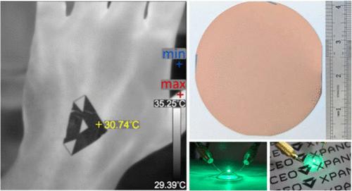
As the trajectory toward the graphene era continues, there is a compelling need to harness 2D technology further for the transformation of three-dimensional (3D) materials production and applications. Here, we resolve this challenge for one of the most widely utilized 3D materials in modern electronics─gold─using graphene-inspired fabrication technology that allows us to develop a multistep production method of ultrathin gold films. Such films demonstrate continuous morphology, low sheet resistance (10 Ω/sq), and high transparency (80%), offering opportunities in a variety of technological and scientific sectors. To this end, we demonstrate smart contact lenses and thermal camouflage based on ultrathin gold. Technologically, the record-breaking characteristics of ultrathin gold films open new horizons for flexible and transparent electrodes for photonics and optoelectronics. Most importantly, the demonstration of transferable wafer-scale ultrathin gold changes the paradigm of the field of 2D crystals and dramatically expands the range of available quasi-2D materials.
石墨烯激发的晶圆级超薄金薄膜
随着石墨烯时代的持续发展,迫切需要进一步利用二维技术来转变三维(3D)材料的生产和应用。在这里,我们使用石墨烯启发的制造技术解决了现代电子产品中应用最广泛的3D材料之一──金──的这一挑战,该技术使我们能够开发出超薄金薄膜的多步骤生产方法。这种薄膜表现出连续的形态,低片阻(10 Ω/sq)和高透明度(80%),为各种技术和科学领域提供了机会。为此,我们展示了智能隐形眼镜和基于超薄黄金的热伪装。在技术上,超薄金薄膜的破纪录特性为光子学和光电子学的柔性和透明电极开辟了新的视野。最重要的是,可转移的晶圆级超薄金的演示改变了二维晶体领域的范式,并极大地扩展了可用的准二维材料的范围。
本文章由计算机程序翻译,如有差异,请以英文原文为准。
求助全文
约1分钟内获得全文
求助全文
来源期刊

Nano Letters
工程技术-材料科学:综合
CiteScore
16.80
自引率
2.80%
发文量
1182
审稿时长
1.4 months
期刊介绍:
Nano Letters serves as a dynamic platform for promptly disseminating original results in fundamental, applied, and emerging research across all facets of nanoscience and nanotechnology. A pivotal criterion for inclusion within Nano Letters is the convergence of at least two different areas or disciplines, ensuring a rich interdisciplinary scope. The journal is dedicated to fostering exploration in diverse areas, including:
- Experimental and theoretical findings on physical, chemical, and biological phenomena at the nanoscale
- Synthesis, characterization, and processing of organic, inorganic, polymer, and hybrid nanomaterials through physical, chemical, and biological methodologies
- Modeling and simulation of synthetic, assembly, and interaction processes
- Realization of integrated nanostructures and nano-engineered devices exhibiting advanced performance
- Applications of nanoscale materials in living and environmental systems
Nano Letters is committed to advancing and showcasing groundbreaking research that intersects various domains, fostering innovation and collaboration in the ever-evolving field of nanoscience and nanotechnology.
 求助内容:
求助内容: 应助结果提醒方式:


