Exploring substrate and Structure-Induced ultrafast phonon dynamics in Bi2Te3 thin films
IF 6.3
2区 材料科学
Q2 CHEMISTRY, PHYSICAL
引用次数: 0
Abstract
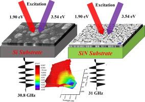
The investigation of phonon and charge carrier dynamics in Bi2Te3 overlayers requires consideration of key factors such as substrate orientation, annealing-induced modifications, and lattice mismatch, emphasizing the need for employing a range of substrates. In this study, Bi2Te3 thin films were grown on Silicon (Si) and Silicon nitride (SiN) substrates under room temperature and annealed conditions. Despite identical growth conditions, significant differences in film morphology were observed due to substrate orientation and lattice mismatch. Morphology due to annealing processes affected the vibration modes of Bi2Te3 and coherent acoustic phonon oscillations in the NIR range. Annealing altered phonon frequencies, leading to oscillation disappearance, attributed to breaking quintuple layers and reforming crystallographic planes, reducing crystallite size. For the as-grown samples, the crystallite size is 19.8 nm for Si and 38.9 nm for SiN, with a respective phonon frequency of 30.8 GHz and 31.3 GHz. After annealing, the morphology changed, reducing the crystallite size to 2.34 nm for Si and 0.54 nm for SiN, respectively. The reduction of crystallite size highly influenced the phonon frequency of Bi2Te3, which has implications for various optoelectronics applications, including tunable frequency generators and GHz-range radar applications.


Bi2Te3薄膜中衬底和结构诱导的超快声子动力学研究
研究Bi2Te3覆盖层中的声子和载流子动力学需要考虑衬底取向、退火诱导修饰和晶格失配等关键因素,强调需要采用一系列衬底。本研究在室温和退火条件下,在硅(Si)和氮化硅(SiN)衬底上生长了Bi2Te3薄膜。在相同的生长条件下,由于衬底取向和晶格不匹配,观察到薄膜形态的显著差异。退火过程的形貌影响了Bi2Te3的振动模式和近红外范围内的相干声子振荡。退火改变了声子频率,导致振荡消失,这是由于五层断裂和重组晶体平面,减少了晶体尺寸。对于生长样品,Si和SiN的晶粒尺寸分别为19.8 nm和38.9 nm,声子频率分别为30.8 GHz和31.3 GHz。退火后,形貌发生变化,Si和SiN的晶粒尺寸分别减小到2.34 nm和0.54 nm。晶体尺寸的减小极大地影响了Bi2Te3的声子频率,这对各种光电子应用具有重要意义,包括可调谐频率发生器和ghz范围雷达应用。
本文章由计算机程序翻译,如有差异,请以英文原文为准。
求助全文
约1分钟内获得全文
求助全文
来源期刊

Applied Surface Science
工程技术-材料科学:膜
CiteScore
12.50
自引率
7.50%
发文量
3393
审稿时长
67 days
期刊介绍:
Applied Surface Science covers topics contributing to a better understanding of surfaces, interfaces, nanostructures and their applications. The journal is concerned with scientific research on the atomic and molecular level of material properties determined with specific surface analytical techniques and/or computational methods, as well as the processing of such structures.
 求助内容:
求助内容: 应助结果提醒方式:


