High-performance InGaZnO/Ga2O3 heterostructure TFTs Gated by high-k Ta1.0La0.4O3.8 fabricated at room temperature
IF 6.9
2区 材料科学
Q2 CHEMISTRY, PHYSICAL
引用次数: 0
Abstract
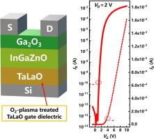
High-performance indium-gallium-zinc-oxide (InGaZnO)/gallium oxide (Ga2O3) heterostructure thin-film transistors (TFTs) featuring high-k tantalum-lanthanum-oxide (TaLaO) gate dielectric have been successfully fabricated via room-temperature sputtering. As investigated by atomic force microscopy (AFM) and x-ray photoelectron spectroscopy (XPS), the high-k Ta1.0La0.4O3.8 can be effectively smoothened by post-deposition plasma treatments at room temperature, suppressing interfacial defects of oxygen vacancies to improve interfacial quality. Remarkably, the electrical characteristics of the heterostructure TFTs are significantly improved by the O2-plasma treatment to yield an ultralow subthreshold swing (SS) of 82.1 mV/dec, an ultrahigh on/off ratio (ION/IOFF) of 4.1 × 10¹⁰, and a high field-effect mobility (µFE) of 68.0 cm2/V·s. This work presents an innovative method that is effective, ultralow-thermal-budget, and cost-efficient for high-performance heterostructure TFTs with high-k gate dielectrics.

室温制备高k Ta1.0La0.4O3.8门控的高性能InGaZnO/Ga2O3异质结构TFTs
采用室温溅射技术成功制备了具有高k钽镧氧化物(TaLaO)栅极介质的高性能铟镓锌氧化物(InGaZnO)/氧化镓(Ga2O3)异质结构薄膜晶体管(TFTs)。原子力显微镜(AFM)和x射线光电子能谱(XPS)研究表明,在室温下,通过沉积后等离子体处理可以有效地平滑高k Ta1.0La0.4O3.8,抑制氧空位的界面缺陷,提高界面质量。值得注意的是,o2等离子体处理显著改善了异质结构tft的电学特性,产生了82.1 mV/dec的超低亚阈值摆幅(SS), 4.1 × 10¹⁰的超高开/关比(ION/IOFF)和68.0 cm2/V·s的高场效应迁移率(µFE)。这项工作提出了一种高效、超低热预算和成本效益的创新方法,用于具有高k栅极电介质的高性能异质结构tft。
本文章由计算机程序翻译,如有差异,请以英文原文为准。
求助全文
约1分钟内获得全文
求助全文
来源期刊

Applied Surface Science
工程技术-材料科学:膜
CiteScore
12.50
自引率
7.50%
发文量
3393
审稿时长
67 days
期刊介绍:
Applied Surface Science covers topics contributing to a better understanding of surfaces, interfaces, nanostructures and their applications. The journal is concerned with scientific research on the atomic and molecular level of material properties determined with specific surface analytical techniques and/or computational methods, as well as the processing of such structures.
 求助内容:
求助内容: 应助结果提醒方式:


