Functional metallic circuitries created by laser-activated selective electroless plating for 3D customized electronics
IF 7.6
2区 材料科学
Q1 MATERIALS SCIENCE, MULTIDISCIPLINARY
引用次数: 0
Abstract
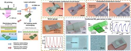
Laser-activated selective electroless plating (LASELP) is a promising complementary manufacturing process employed in hybrid additive manufacturing (HAM) technology for the fabrication of customized 3D electronics. However, to the best knowledge of the authors, most current LASELP technologies could only enable copper deposition on/within the polymer matrix, which largely limited the application scope of this technology. Accordingly, an advanced LASELP technology combining catalyst exchanging process is proposed to pattern diverse functional metals on the photopolymer to fabricate 3D electronics. Two kinds of catalyst systems are selected in this HAM technology: (1) Cu2(OH)PO4; (2) antimony tin oxide (ATO) and titania (TiO2). Silver and nickel-phosphorus (Ni-P) alloy are selected as the representatives of direct- and indirect-ELP metals, respectively. Silver could be directly plated on the laser-activated surface to deposit a dense and highly conductive layer, while for the Ni-P layer an inevitable catalyst exchange step is applied here to induce Pd0 plating seeds on the laser-activated substrate. Finally, a variety of customized electronics, such as conformal circuit boards, smart structure with strain sensor, embedded structural thermometer, Internet of Things bottle cap, and gas tube integrated with 3D conformal NO2 sensor are fabricated and fully verify this HAM technology.

功能金属电路创建激光激活选择性化学镀3D定制电子产品
激光活化选择性化学镀(LASELP)是一种很有前途的互补制造工艺,用于制造定制3D电子产品的混合增材制造(HAM)技术。然而,据作者所知,目前大多数LASELP技术只能在聚合物基体上/内部沉积铜,这在很大程度上限制了该技术的应用范围。因此,提出了一种先进的LASELP技术,结合催化剂交换过程,在光聚合物上图案化多种功能金属,以制造3D电子产品。本工艺选用了两种催化剂体系:(1)Cu2(OH)PO4;(2)氧化锑锡(ATO)和二氧化钛(TiO2)。选择银和镍磷(Ni-P)合金分别作为直接和间接elp金属的代表。将银直接镀在激光激活表面,形成致密的高导电性镀层,而对于Ni-P层,则必须通过催化剂交换步骤在激光激活的衬底上诱导Pd0电镀种子。最后,制作了各种定制电子产品,如共形电路板,带应变传感器的智能结构,嵌入式结构温度计,物联网瓶盖和集成3D共形NO2传感器的气管,并充分验证了该HAM技术。
本文章由计算机程序翻译,如有差异,请以英文原文为准。
求助全文
约1分钟内获得全文
求助全文
来源期刊

Materials & Design
Engineering-Mechanical Engineering
CiteScore
14.30
自引率
7.10%
发文量
1028
审稿时长
85 days
期刊介绍:
Materials and Design is a multi-disciplinary journal that publishes original research reports, review articles, and express communications. The journal focuses on studying the structure and properties of inorganic and organic materials, advancements in synthesis, processing, characterization, and testing, the design of materials and engineering systems, and their applications in technology. It aims to bring together various aspects of materials science, engineering, physics, and chemistry.
The journal explores themes ranging from materials to design and aims to reveal the connections between natural and artificial materials, as well as experiment and modeling. Manuscripts submitted to Materials and Design should contain elements of discovery and surprise, as they often contribute new insights into the architecture and function of matter.
 求助内容:
求助内容: 应助结果提醒方式:


