Area-Selective Molecular Layer Deposition of Alucone on Photoresist for Enhanced Pattern Transfer
IF 7.2
2区 材料科学
Q2 CHEMISTRY, PHYSICAL
引用次数: 0
Abstract
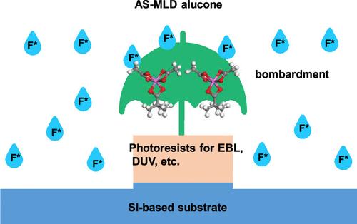
Multilayer mask dry etching is commonly used for pattern transfer on industrial lines to reduce the semiconductor component size. One of the challenges is the need for improved photoresists (PRs) that combine high resolution and etch selectivity with low complexity and material cost. Here, an alternative masking approach using area-selective molecular layer deposition (AS-MLD) has been shown to improve the etch resistance and pattern transfer accuracy. This technology enables the selective deposition of alucone into prepatterned PR areas or a class of PRs rich in ester groups like poly(methyl methacrylate) (PMMA), avoiding the deposition on the silicon-based substrate. The AS-MLD minimizes feature size variation and reduces edge placement errors. In this work, the mechanism of selective deposition of alucone on PMMA and the inhibition mechanism on Si-based substrates were investigated in detail. The alucone-PMMA demonstrates considerable resistance to high-energy fluorine plasma etching. Compared to the original PMMA, the etch resistance is improved by 85 times and the etch selectivity between alucone-PMMA-trimmed and SiON or SiO2 can reach as high as 52 or 32, respectively. By improving film uniformity and thickness control, this method simplifies the manufacturing process, increases production efficiency, and reduces costs. Our approach addresses the urgent need for improved deposition selectivity and resolution in extreme ultraviolet (EUV) lithography and is an important step toward achieving reliable and high-performance semiconductor devices.

求助全文
约1分钟内获得全文
求助全文
来源期刊

Chemistry of Materials
工程技术-材料科学:综合
CiteScore
14.10
自引率
5.80%
发文量
929
审稿时长
1.5 months
期刊介绍:
The journal Chemistry of Materials focuses on publishing original research at the intersection of materials science and chemistry. The studies published in the journal involve chemistry as a prominent component and explore topics such as the design, synthesis, characterization, processing, understanding, and application of functional or potentially functional materials. The journal covers various areas of interest, including inorganic and organic solid-state chemistry, nanomaterials, biomaterials, thin films and polymers, and composite/hybrid materials. The journal particularly seeks papers that highlight the creation or development of innovative materials with novel optical, electrical, magnetic, catalytic, or mechanical properties. It is essential that manuscripts on these topics have a primary focus on the chemistry of materials and represent a significant advancement compared to prior research. Before external reviews are sought, submitted manuscripts undergo a review process by a minimum of two editors to ensure their appropriateness for the journal and the presence of sufficient evidence of a significant advance that will be of broad interest to the materials chemistry community.
 求助内容:
求助内容: 应助结果提醒方式:


