Enhancing MoS2 Electronic Performance with Solid-State Lithium-Ion Electrolyte Contacts through Dielectric Screening
IF 15.8
1区 材料科学
Q1 CHEMISTRY, MULTIDISCIPLINARY
引用次数: 0
Abstract
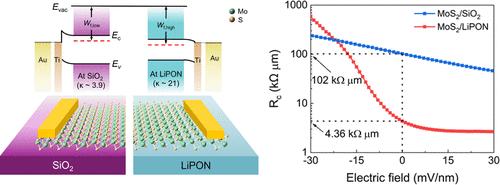
The high electrical contact resistance at the metal–semiconductor interface hinders the practical application of two-dimensional (2D) semiconductor electronics in the postsilicon era. Conventional strategies toward Ohmic contact involve optimizing contact electrode materials. In this work, we utilize the band structure tunability of a 2D semiconductor by introducing a high dielectric constant gate dielectric to optimize the Schottky barrier height and width. Here, the dielectric screening effect induced by a solid-state lithium-ion electrolyte significantly reduces the Schottky barrier height to 2.7 meV. The resulting MoS2 transistor achieves a subthreshold swing of 84 mV/dev and a drastically reduced contact resistance of 4.36 kΩ μm. The contact properties of the device under operational conditions are studied by in situ Kelvin probe force microscopy. Furthermore, the device demonstrates promising photodetection capabilities for visible and near-infrared light along with a fast response time. This work presents an approach to enhancing dielectric contacts in 2D semiconductors for advancing high-performance electronic and optoelectronic devices.

通过介质筛选提高固态锂离子电解质触点MoS2电子性能
金属-半导体界面处的高电接触电阻阻碍了后硅时代二维半导体电子的实际应用。传统的欧姆接触策略包括优化接触电极材料。在这项工作中,我们通过引入高介电常数栅极电介质来利用二维半导体的带结构可调性来优化肖特基势垒的高度和宽度。在这里,固态锂离子电解质诱导的介电屏蔽效应显著降低了肖特基势垒高度至2.7 meV。由此得到的MoS2晶体管实现了84 mV/dev的亚阈值摆幅,并大幅降低了4.36 kΩ μm的接触电阻。用原位开尔文探针力显微镜研究了器件在工作条件下的接触特性。此外,该装置还展示了对可见光和近红外光的有前途的光探测能力,以及快速的响应时间。这项工作提出了一种增强二维半导体介质接触的方法,用于推进高性能电子和光电子器件。
本文章由计算机程序翻译,如有差异,请以英文原文为准。
求助全文
约1分钟内获得全文
求助全文
来源期刊

ACS Nano
工程技术-材料科学:综合
CiteScore
26.00
自引率
4.10%
发文量
1627
审稿时长
1.7 months
期刊介绍:
ACS Nano, published monthly, serves as an international forum for comprehensive articles on nanoscience and nanotechnology research at the intersections of chemistry, biology, materials science, physics, and engineering. The journal fosters communication among scientists in these communities, facilitating collaboration, new research opportunities, and advancements through discoveries. ACS Nano covers synthesis, assembly, characterization, theory, and simulation of nanostructures, nanobiotechnology, nanofabrication, methods and tools for nanoscience and nanotechnology, and self- and directed-assembly. Alongside original research articles, it offers thorough reviews, perspectives on cutting-edge research, and discussions envisioning the future of nanoscience and nanotechnology.
 求助内容:
求助内容: 应助结果提醒方式:


