Simulation and optimization of reactor airflow and magnetic field for enhanced thin film uniformity in physical vapor deposition
IF 3.1
4区 工程技术
Q2 ENGINEERING, ELECTRICAL & ELECTRONIC
引用次数: 0
Abstract
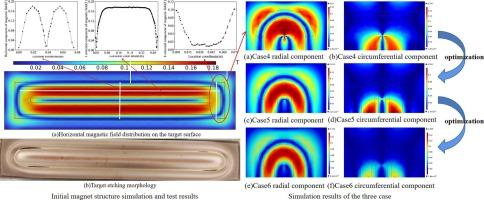
Planar magnetron sputtering reactors are widely utilized in the semiconductor industry due to their high deposition rate, low substrate temperature, and capability for large-area coating. Careful control of the reactor's flow field and magnetic field is essential to ensure appropriate thickness uniformity of the thin film and uniform etching of the target. Utilizing finite element analysis software, simulations were conducted to obtain numerical solutions for the airflow and magnetic field. An increase in the inlet diameter from 4 mm to 5 mm resulted in a 63.4 % decrease in the gas distribution unevenness coefficient. Conversely, increasing the outlet diameter from 1 mm to 2 mm led to a 636.6 % increase in the coefficient. At a pitch of 11.7 mm, the horizontal magnetic field component on the target surface peaked at 0.24 T, covering a larger area. A dual-runway structure reduced the circumferential component of the horizontal magnetic field by more than half. Analysis of the results precipitated the optimization of key component structures, resulting in an optimal solution: an air ring diameter of 5 mm, an outlet diameter of 1 mm, outlet spacing of 12 mm, double inlets, and 38 outlets on each side of the air ring. Further optimization determined the optimal magnet-to-target surface spacing of 11.7 mm, with the dual-runway structure effectively improving the uniformity of the radial magnetic field distribution and increasing the target etching area. This study provides a theoretical basis for optimizing planar magnetron sputtering reactors.

模拟和优化反应器气流和磁场,提高物理气相沉积过程中的薄膜均匀性
平面磁控溅射反应器因其高沉积率、低基底温度和大面积镀膜能力而广泛应用于半导体行业。对反应器流场和磁场的精心控制对于确保适当的薄膜厚度均匀性和靶材的均匀蚀刻至关重要。利用有限元分析软件进行了模拟,以获得气流和磁场的数值解。进气口直径从 4 毫米增加到 5 毫米后,气体分布不均匀系数降低了 63.4%。相反,将出口直径从 1 毫米增加到 2 毫米,该系数增加了 636.6%。当间距为 11.7 毫米时,目标表面的水平磁场分量达到 0.24 T 的峰值,覆盖面积更大。双通道结构将水平磁场的圆周分量减少了一半以上。对结果进行分析后,对关键部件结构进行了优化,最终确定了一个最佳解决方案:空气环直径为 5 毫米,出气口直径为 1 毫米,出气口间距为 12 毫米,双进气口,空气环两侧各有 38 个出气口。进一步优化确定的最佳磁铁与目标表面间距为 11.7 毫米,双通道结构有效改善了径向磁场分布的均匀性,并增加了目标蚀刻面积。这项研究为优化平面磁控溅射反应器提供了理论依据。
本文章由计算机程序翻译,如有差异,请以英文原文为准。
求助全文
约1分钟内获得全文
求助全文
来源期刊

Microelectronic Engineering
工程技术-工程:电子与电气
CiteScore
5.30
自引率
4.30%
发文量
131
审稿时长
29 days
期刊介绍:
Microelectronic Engineering is the premier nanoprocessing, and nanotechnology journal focusing on fabrication of electronic, photonic, bioelectronic, electromechanic and fluidic devices and systems, and their applications in the broad areas of electronics, photonics, energy, life sciences, and environment. It covers also the expanding interdisciplinary field of "more than Moore" and "beyond Moore" integrated nanoelectronics / photonics and micro-/nano-/bio-systems. Through its unique mixture of peer-reviewed articles, reviews, accelerated publications, short and Technical notes, and the latest research news on key developments, Microelectronic Engineering provides comprehensive coverage of this exciting, interdisciplinary and dynamic new field for researchers in academia and professionals in industry.
 求助内容:
求助内容: 应助结果提醒方式:


