The effects of growth interruptions in the GaAsBi/InAs/GaAs quantum dots: The emergence of three-phase nanoparticles

IF 5.7 2区 材料科学 Q2 CHEMISTRY, PHYSICAL
S. Flores , D.F. Reyes , V. Braza , N.J. Bailey , M.R. Carr , R.D. Richards , D. Gonzalez
{"title":"The effects of growth interruptions in the GaAsBi/InAs/GaAs quantum dots: The emergence of three-phase nanoparticles","authors":"S. Flores ,&nbsp;D.F. Reyes ,&nbsp;V. Braza ,&nbsp;N.J. Bailey ,&nbsp;M.R. Carr ,&nbsp;R.D. Richards ,&nbsp;D. Gonzalez","doi":"10.1016/j.surfin.2024.105490","DOIUrl":null,"url":null,"abstract":"<div><div>The study investigated the impact of introducing bismuth into the GaAs capping layer (CL) on InAs quantum dots (QDs) to enhance their QD properties. Three different time-temperature routes (TTRs) were examined, as growth interruption (GI) stages are necessary due to the temperature requirements for the growth processes of QDs (510 °C) and GaAsBi CL (370 °C). Two of the TTRs revealed defective regions with bismuth-free nanotracks in the GaAsBi CL, which are linked to the formation of bismuth-rich droplets on the surface. Interestingly, in one of the TTRs, novel icosahedral-type nanoparticles appeared embedded at the first interface, leaving trails behind them. Upon detailed characterization, it was found that these nanoparticles consist of three distinct phases containing rhombohedral Bi, pure Ga, and a new In<sub>4</sub>Bi phase that had not been experimentally described before. The long particle trajectories and low temperatures suggest that the NPs remained liquid throughout the growth process, solidifying upon final cooling to room temperature. This work presents a new technique for incorporating plasmonic nanoparticle arrays made of non-noble metals into buried semiconductor layered interfaces, which offers greater flexibility in device design.</div></div>","PeriodicalId":22081,"journal":{"name":"Surfaces and Interfaces","volume":"56 ","pages":"Article 105490"},"PeriodicalIF":5.7000,"publicationDate":"2024-11-22","publicationTypes":"Journal Article","fieldsOfStudy":null,"isOpenAccess":false,"openAccessPdf":"","citationCount":"0","resultStr":null,"platform":"Semanticscholar","paperid":null,"PeriodicalName":"Surfaces and Interfaces","FirstCategoryId":"88","ListUrlMain":"https://www.sciencedirect.com/science/article/pii/S2468023024016468","RegionNum":2,"RegionCategory":"材料科学","ArticlePicture":[],"TitleCN":null,"AbstractTextCN":null,"PMCID":null,"EPubDate":"","PubModel":"","JCR":"Q2","JCRName":"CHEMISTRY, PHYSICAL","Score":null,"Total":0}
引用次数: 0

Abstract

The study investigated the impact of introducing bismuth into the GaAs capping layer (CL) on InAs quantum dots (QDs) to enhance their QD properties. Three different time-temperature routes (TTRs) were examined, as growth interruption (GI) stages are necessary due to the temperature requirements for the growth processes of QDs (510 °C) and GaAsBi CL (370 °C). Two of the TTRs revealed defective regions with bismuth-free nanotracks in the GaAsBi CL, which are linked to the formation of bismuth-rich droplets on the surface. Interestingly, in one of the TTRs, novel icosahedral-type nanoparticles appeared embedded at the first interface, leaving trails behind them. Upon detailed characterization, it was found that these nanoparticles consist of three distinct phases containing rhombohedral Bi, pure Ga, and a new In4Bi phase that had not been experimentally described before. The long particle trajectories and low temperatures suggest that the NPs remained liquid throughout the growth process, solidifying upon final cooling to room temperature. This work presents a new technique for incorporating plasmonic nanoparticle arrays made of non-noble metals into buried semiconductor layered interfaces, which offers greater flexibility in device design.
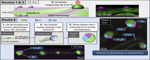
Abstract Image

GaAsBi/InAs/GaAs 量子点生长中断的影响:三相纳米粒子的出现
该研究调查了在砷化镓封盖层(CL)中引入铋对砷化镓量子点(QD)的影响,以增强其 QD 特性。由于 QDs(510 °C)和 GaAsBi CL(370 °C)生长过程的温度要求,生长中断(GI)阶段是必要的,因此研究人员考察了三种不同的时间-温度路线(TTR)。其中两个 TTR 显示了 GaAsBi CL 中无铋纳米轨道的缺陷区域,这与表面富铋液滴的形成有关。有趣的是,在其中一个 TTR 中,新的二十面体型纳米粒子出现在第一个界面上,并在后面留下了痕迹。经过详细表征,发现这些纳米粒子由三个不同的相组成,包括斜方体 Bi 相、纯镓相和一种新的 In4Bi 相,而这种新的 In4Bi 相以前从未在实验中描述过。粒子的长轨迹和低温表明,纳米粒子在整个生长过程中保持液态,并在最终冷却至室温后凝固。这项研究提出了一种将非贵金属质子纳米粒子阵列纳入埋入式半导体层界面的新技术,为器件设计提供了更大的灵活性。
本文章由计算机程序翻译,如有差异,请以英文原文为准。
求助全文
约1分钟内获得全文 求助全文
来源期刊
Surfaces and Interfaces
Surfaces and Interfaces Chemistry-General Chemistry
CiteScore
8.50
自引率
6.50%
发文量
753
审稿时长
35 days
期刊介绍: The aim of the journal is to provide a respectful outlet for ''sound science'' papers in all research areas on surfaces and interfaces. We define sound science papers as papers that describe new and well-executed research, but that do not necessarily provide brand new insights or are merely a description of research results. Surfaces and Interfaces publishes research papers in all fields of surface science which may not always find the right home on first submission to our Elsevier sister journals (Applied Surface, Surface and Coatings Technology, Thin Solid Films)
×
引用
GB/T 7714-2015
复制
MLA
复制
APA
复制
导出至
BibTeX EndNote RefMan NoteFirst NoteExpress
×
提示
您的信息不完整,为了账户安全,请先补充。
现在去补充
×
提示
您因"违规操作"
具体请查看互助需知
我知道了
×
提示
确定
请完成安全验证×
copy
已复制链接
快去分享给好友吧!
我知道了
右上角分享
点击右上角分享
0
联系我们:info@booksci.cn Book学术提供免费学术资源搜索服务,方便国内外学者检索中英文文献。致力于提供最便捷和优质的服务体验。 Copyright © 2023 布克学术 All rights reserved.
京ICP备2023020795号-1
ghs 京公网安备 11010802042870号
Book学术文献互助
Book学术文献互助群
群 号:481959085
Book学术官方微信