Resolving the Electron Plume within a Scanning Electron Microscope

IF 15.8 1区 材料科学 Q1 CHEMISTRY, MULTIDISCIPLINARY
ACS Nano Pub Date : 2024-11-27 DOI:10.1021/acsnano.4c10527
Francis M. Alcorn, Christopher Perez, Eric J. Smoll, Lauren Hoang, Frederick U. Nitta, Andrew J. Mannix, A. Alec Talin, Craig Y. Nakakura, David W. Chandler, Suhas Kumar
{"title":"Resolving the Electron Plume within a Scanning Electron Microscope","authors":"Francis M. Alcorn, Christopher Perez, Eric J. Smoll, Lauren Hoang, Frederick U. Nitta, Andrew J. Mannix, A. Alec Talin, Craig Y. Nakakura, David W. Chandler, Suhas Kumar","doi":"10.1021/acsnano.4c10527","DOIUrl":null,"url":null,"abstract":"Scanning electron microscopy (SEM), a century-old technique, is today a ubiquitous method of imaging the surface of nanostructures. However, most SEM detectors simply count the number of secondary electrons from a material of interest, and thereby overlook the rich material information contained within them. Here, by simple modifications to a standard SEM tool, we resolve the momentum and energy information on secondary electrons by directly imaging the electron plume generated by the electron beam of the SEM. Leveraging these spectroscopic imaging capabilities, our technique is able to image lateral electric fields across a prototypical silicon p–n junctions and to distinguish differently doped regions, even when buried beyond depths typically accessible by SEM. Intriguingly, the subsurface sensitivity of this technique reveals unexpectedly strong surface band bending within nominally passivated semiconductor structures, providing useful insights for complex layered component designs, in which interfacial dynamics dictate device operation. These capabilities for noninvasive, multimodal probing of complicated electronic components are crucial in today’s electronic manufacturing but is largely inaccessible even with sophisticated techniques. These results show that seemingly simple SEM can be extended to probe complex and useful material properties.","PeriodicalId":21,"journal":{"name":"ACS Nano","volume":"258 1","pages":""},"PeriodicalIF":15.8000,"publicationDate":"2024-11-27","publicationTypes":"Journal Article","fieldsOfStudy":null,"isOpenAccess":false,"openAccessPdf":"","citationCount":"0","resultStr":null,"platform":"Semanticscholar","paperid":null,"PeriodicalName":"ACS Nano","FirstCategoryId":"88","ListUrlMain":"https://doi.org/10.1021/acsnano.4c10527","RegionNum":1,"RegionCategory":"材料科学","ArticlePicture":[],"TitleCN":null,"AbstractTextCN":null,"PMCID":null,"EPubDate":"","PubModel":"","JCR":"Q1","JCRName":"CHEMISTRY, MULTIDISCIPLINARY","Score":null,"Total":0}
引用次数: 0

Abstract

Scanning electron microscopy (SEM), a century-old technique, is today a ubiquitous method of imaging the surface of nanostructures. However, most SEM detectors simply count the number of secondary electrons from a material of interest, and thereby overlook the rich material information contained within them. Here, by simple modifications to a standard SEM tool, we resolve the momentum and energy information on secondary electrons by directly imaging the electron plume generated by the electron beam of the SEM. Leveraging these spectroscopic imaging capabilities, our technique is able to image lateral electric fields across a prototypical silicon p–n junctions and to distinguish differently doped regions, even when buried beyond depths typically accessible by SEM. Intriguingly, the subsurface sensitivity of this technique reveals unexpectedly strong surface band bending within nominally passivated semiconductor structures, providing useful insights for complex layered component designs, in which interfacial dynamics dictate device operation. These capabilities for noninvasive, multimodal probing of complicated electronic components are crucial in today’s electronic manufacturing but is largely inaccessible even with sophisticated techniques. These results show that seemingly simple SEM can be extended to probe complex and useful material properties.
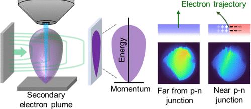
Abstract Image

在扫描电子显微镜内分辨电子羽流
扫描电子显微镜(SEM)是一项具有百年历史的技术,如今已成为纳米结构表面成像的普遍方法。然而,大多数扫描电子显微镜探测器只是简单地计算相关材料的二次电子数量,从而忽略了其中包含的丰富材料信息。在这里,我们对标准扫描电子显微镜工具进行了简单的改装,通过对扫描电子显微镜电子束产生的电子羽流直接成像,解析了二次电子的动量和能量信息。利用这些光谱成像功能,我们的技术能够对原型硅 p-n 结的横向电场进行成像,并区分不同的掺杂区域,即使埋藏深度超出了扫描电子显微镜通常可以触及的范围。耐人寻味的是,这项技术的表层下灵敏度揭示了名义上钝化的半导体结构中出乎意料的强烈表面带弯曲,为复杂的分层元件设计提供了有用的见解,在这种设计中,界面动力学决定了器件的运行。这些对复杂电子元件进行非侵入式、多模态探测的能力对当今的电子制造至关重要,但即使采用先进的技术也很难实现。这些结果表明,看似简单的扫描电子显微镜可以扩展到探测复杂而有用的材料特性。
本文章由计算机程序翻译,如有差异,请以英文原文为准。
求助全文
约1分钟内获得全文 求助全文
来源期刊
ACS Nano
ACS Nano 工程技术-材料科学:综合
CiteScore
26.00
自引率
4.10%
发文量
1627
审稿时长
1.7 months
期刊介绍: ACS Nano, published monthly, serves as an international forum for comprehensive articles on nanoscience and nanotechnology research at the intersections of chemistry, biology, materials science, physics, and engineering. The journal fosters communication among scientists in these communities, facilitating collaboration, new research opportunities, and advancements through discoveries. ACS Nano covers synthesis, assembly, characterization, theory, and simulation of nanostructures, nanobiotechnology, nanofabrication, methods and tools for nanoscience and nanotechnology, and self- and directed-assembly. Alongside original research articles, it offers thorough reviews, perspectives on cutting-edge research, and discussions envisioning the future of nanoscience and nanotechnology.
×
引用
GB/T 7714-2015
复制
MLA
复制
APA
复制
导出至
BibTeX EndNote RefMan NoteFirst NoteExpress
×
提示
您的信息不完整,为了账户安全,请先补充。
现在去补充
×
提示
您因"违规操作"
具体请查看互助需知
我知道了
×
提示
确定
请完成安全验证×
copy
已复制链接
快去分享给好友吧!
我知道了
右上角分享
点击右上角分享
0
联系我们:info@booksci.cn Book学术提供免费学术资源搜索服务,方便国内外学者检索中英文文献。致力于提供最便捷和优质的服务体验。 Copyright © 2023 布克学术 All rights reserved.
京ICP备2023020795号-1
ghs 京公网安备 11010802042870号
Book学术文献互助
Book学术文献互助群
群 号:481959085
Book学术官方微信