Asraful Haque, Suman Kumar Mandal, Shubham Kumar Parate, Harshal Jason D′souza, Pavan Nukala and Srinivasan Raghavan
{"title":"Free standing epitaxial oxides through remote epitaxy: the role of the evolving graphene microstructure†","authors":"Asraful Haque, Suman Kumar Mandal, Shubham Kumar Parate, Harshal Jason D′souza, Pavan Nukala and Srinivasan Raghavan","doi":"10.1039/D4NR03356F","DOIUrl":null,"url":null,"abstract":"<p >Remote epitaxy has garnered considerable attention as a promising method that facilitates the growth of thin films that replicate the crystallographic characteristics of a substrate by utilizing two-dimensional (2D) material interlayers such as graphene. The resulting film can be exfoliated to form a freestanding membrane and the substrate, if expensive, can be reused. However, atomically thin 2D materials are susceptible to damage before and during film growth in the chamber, leading to poor epitaxy. Oxide remote epitaxy using graphene, the most commonly available 2D material, is particularly challenging because the conventional conditions employed for the growth of epitaxial oxides also degrade graphene. In this study, we show for the first time that a direct correlation exists between the microstructure of graphene, the graphene becoming defective upon exposure to the pulsed laser deposition plume and the crystalline quality of the BaTiO<small><sub>3</sub></small> (BTO) film deposited on top. A controlled aperture method was used to reduce graphene damage. Even so, the degree of damage is more at the graphene grain boundaries than within the grains. Graphene with a large grain size of >300 microns suffered less damage and yielded a film comparable to that grown directly on a SrTiO<small><sub>3</sub></small> (STO) substrate with a rocking curve half width of 0.6°. Using large grain sized bi-layer graphene, 4 mm × 5 mm oxide layers were successfully exfoliated and transferred onto SiO<small><sub><em>x</em></sub></small>–Si. These insights pave the way for the heterogeneous integration of functional oxides on foreign substrates, holding significant implications for commercializing perovskite oxides by integrating them with Si-CMOS and flexible electronics.</p>","PeriodicalId":92,"journal":{"name":"Nanoscale","volume":" 4","pages":" 2020-2031"},"PeriodicalIF":5.1000,"publicationDate":"2024-11-27","publicationTypes":"Journal Article","fieldsOfStudy":null,"isOpenAccess":false,"openAccessPdf":"","citationCount":"0","resultStr":null,"platform":"Semanticscholar","paperid":null,"PeriodicalName":"Nanoscale","FirstCategoryId":"88","ListUrlMain":"https://pubs.rsc.org/en/content/articlelanding/2025/nr/d4nr03356f","RegionNum":3,"RegionCategory":"材料科学","ArticlePicture":[],"TitleCN":null,"AbstractTextCN":null,"PMCID":null,"EPubDate":"","PubModel":"","JCR":"Q1","JCRName":"CHEMISTRY, MULTIDISCIPLINARY","Score":null,"Total":0}
引用次数: 0
Abstract
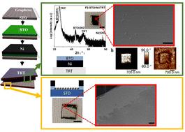
Remote epitaxy has garnered considerable attention as a promising method that facilitates the growth of thin films that replicate the crystallographic characteristics of a substrate by utilizing two-dimensional (2D) material interlayers such as graphene. The resulting film can be exfoliated to form a freestanding membrane and the substrate, if expensive, can be reused. However, atomically thin 2D materials are susceptible to damage before and during film growth in the chamber, leading to poor epitaxy. Oxide remote epitaxy using graphene, the most commonly available 2D material, is particularly challenging because the conventional conditions employed for the growth of epitaxial oxides also degrade graphene. In this study, we show for the first time that a direct correlation exists between the microstructure of graphene, the graphene becoming defective upon exposure to the pulsed laser deposition plume and the crystalline quality of the BaTiO3 (BTO) film deposited on top. A controlled aperture method was used to reduce graphene damage. Even so, the degree of damage is more at the graphene grain boundaries than within the grains. Graphene with a large grain size of >300 microns suffered less damage and yielded a film comparable to that grown directly on a SrTiO3 (STO) substrate with a rocking curve half width of 0.6°. Using large grain sized bi-layer graphene, 4 mm × 5 mm oxide layers were successfully exfoliated and transferred onto SiOx–Si. These insights pave the way for the heterogeneous integration of functional oxides on foreign substrates, holding significant implications for commercializing perovskite oxides by integrating them with Si-CMOS and flexible electronics.
期刊介绍:
Nanoscale is a high-impact international journal, publishing high-quality research across nanoscience and nanotechnology. Nanoscale publishes a full mix of research articles on experimental and theoretical work, including reviews, communications, and full papers.Highly interdisciplinary, this journal appeals to scientists, researchers and professionals interested in nanoscience and nanotechnology, quantum materials and quantum technology, including the areas of physics, chemistry, biology, medicine, materials, energy/environment, information technology, detection science, healthcare and drug discovery, and electronics.

 求助内容:
求助内容: 应助结果提醒方式:


