SiO2/Si interface defects in HKMG stack fabrication

IF 5.7 2区 材料科学 Q2 CHEMISTRY, PHYSICAL
Shota Nunomura , Yukinori Morita
{"title":"SiO2/Si interface defects in HKMG stack fabrication","authors":"Shota Nunomura ,&nbsp;Yukinori Morita","doi":"10.1016/j.surfin.2024.105445","DOIUrl":null,"url":null,"abstract":"<div><div>The defect generation and recovery near the silicon dioxide (SiO<sub>2</sub>)/silicon (Si) interface are studied throughout high-k dielectric/metal gate (HKMG) stack fabrication and post-processing. The HKMG stack is prepared on a Si wafer in a well-established manner, using chemical oxidation for an interfacial layer of SiO<sub>2</sub>, atomic layer deposition (ALD) for HK-hafnium oxide (HfO<span><math><msub><mrow></mrow><mrow><mn>2</mn></mrow></msub></math></span>), and magnetron sputtering for MG-tantalum nitride (TaN). The stack is then treated with additional processing of post-deposition annealing (PDA), oxygen (O<span><math><msub><mrow></mrow><mrow><mn>2</mn></mrow></msub></math></span>) plasma processing, and forming gas annealing (FGA) to imitate transistor manufacturing. Throughout these processing, the atomic-level defects near the SiO<sub>2</sub>/Si interface are characterized, with quasi-steady-state photoconductance (QSSPC) measurements. With the measurements, it is found that the defects near the SiO<sub>2</sub>/Si interface are generated by most of the processing of ALD-HfO<span><math><msub><mrow></mrow><mrow><mn>2</mn></mrow></msub></math></span>, sputter-TaN as well as PDA and O<span><math><msub><mrow></mrow><mrow><mn>2</mn></mrow></msub></math></span> plasma, whereas those defects are recovered by the last step of FGA. Interestingly, the recovery of defects depends on the HKMG stack structure and processing; the recovery is highly limited for a thin stack treated with high-temperature PDA. In such a case, residual defects are created near the SiO<sub>2</sub>/Si interface.</div></div>","PeriodicalId":22081,"journal":{"name":"Surfaces and Interfaces","volume":"56 ","pages":"Article 105445"},"PeriodicalIF":5.7000,"publicationDate":"2024-11-20","publicationTypes":"Journal Article","fieldsOfStudy":null,"isOpenAccess":false,"openAccessPdf":"","citationCount":"0","resultStr":null,"platform":"Semanticscholar","paperid":null,"PeriodicalName":"Surfaces and Interfaces","FirstCategoryId":"88","ListUrlMain":"https://www.sciencedirect.com/science/article/pii/S2468023024016018","RegionNum":2,"RegionCategory":"材料科学","ArticlePicture":[],"TitleCN":null,"AbstractTextCN":null,"PMCID":null,"EPubDate":"","PubModel":"","JCR":"Q2","JCRName":"CHEMISTRY, PHYSICAL","Score":null,"Total":0}
引用次数: 0

Abstract

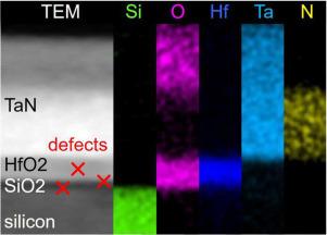
The defect generation and recovery near the silicon dioxide (SiO2)/silicon (Si) interface are studied throughout high-k dielectric/metal gate (HKMG) stack fabrication and post-processing. The HKMG stack is prepared on a Si wafer in a well-established manner, using chemical oxidation for an interfacial layer of SiO2, atomic layer deposition (ALD) for HK-hafnium oxide (HfO2), and magnetron sputtering for MG-tantalum nitride (TaN). The stack is then treated with additional processing of post-deposition annealing (PDA), oxygen (O2) plasma processing, and forming gas annealing (FGA) to imitate transistor manufacturing. Throughout these processing, the atomic-level defects near the SiO2/Si interface are characterized, with quasi-steady-state photoconductance (QSSPC) measurements. With the measurements, it is found that the defects near the SiO2/Si interface are generated by most of the processing of ALD-HfO2, sputter-TaN as well as PDA and O2 plasma, whereas those defects are recovered by the last step of FGA. Interestingly, the recovery of defects depends on the HKMG stack structure and processing; the recovery is highly limited for a thin stack treated with high-temperature PDA. In such a case, residual defects are created near the SiO2/Si interface.
Abstract Image

香港半导体制造堆栈中的二氧化硅/硅界面缺陷
在整个高介电/金属栅极(HKMG)堆栈制造和后处理过程中,对二氧化硅(SiO2)/硅(Si)界面附近的缺陷产生和恢复进行了研究。HKMG 叠层是在硅晶片上以成熟的方式制备的,采用化学氧化法制备二氧化硅界面层,原子层沉积 (ALD) 法制备 HK-氧化铪 (HfO2),磁控溅射法制备 MG-氮化钽 (TaN)。然后对堆栈进行沉积后退火 (PDA)、氧气 (O2) 等离子处理和成型气体退火 (FGA) 等附加处理,以模仿晶体管的制造过程。在整个加工过程中,通过准稳态光电导(QSSPC)测量,对二氧化硅/硅界面附近的原子级缺陷进行了表征。测量结果表明,在 ALD-HfO2、溅射-TaN 以及 PDA 和 O2 等离子体的大部分加工过程中,SiO2/Si 界面附近都会产生缺陷,而这些缺陷会在 FGA 的最后一步得到恢复。有趣的是,缺陷的恢复取决于香港马会开奖结果堆栈的结构和处理过程;对于使用高温 PDA 处理的薄堆栈,缺陷的恢复非常有限。在这种情况下,会在二氧化硅/硅界面附近产生残余缺陷。
本文章由计算机程序翻译,如有差异,请以英文原文为准。
求助全文
约1分钟内获得全文 求助全文
来源期刊
Surfaces and Interfaces
Surfaces and Interfaces Chemistry-General Chemistry
CiteScore
8.50
自引率
6.50%
发文量
753
审稿时长
35 days
期刊介绍: The aim of the journal is to provide a respectful outlet for ''sound science'' papers in all research areas on surfaces and interfaces. We define sound science papers as papers that describe new and well-executed research, but that do not necessarily provide brand new insights or are merely a description of research results. Surfaces and Interfaces publishes research papers in all fields of surface science which may not always find the right home on first submission to our Elsevier sister journals (Applied Surface, Surface and Coatings Technology, Thin Solid Films)
×
引用
GB/T 7714-2015
复制
MLA
复制
APA
复制
导出至
BibTeX EndNote RefMan NoteFirst NoteExpress
×
提示
您的信息不完整,为了账户安全,请先补充。
现在去补充
×
提示
您因"违规操作"
具体请查看互助需知
我知道了
×
提示
确定
请完成安全验证×
copy
已复制链接
快去分享给好友吧!
我知道了
右上角分享
点击右上角分享
0
联系我们:info@booksci.cn Book学术提供免费学术资源搜索服务,方便国内外学者检索中英文文献。致力于提供最便捷和优质的服务体验。 Copyright © 2023 布克学术 All rights reserved.
京ICP备2023020795号-1
ghs 京公网安备 11010802042870号
Book学术文献互助
Book学术文献互助群
群 号:481959085
Book学术官方微信