Patterned dielectric back contact design for GaAs thermophotovoltaic devices

IF 6.3 2区 材料科学 Q2 ENERGY & FUELS
Madhan K. Arulanandam , Jeronimo Buencuerpo , Myles A. Steiner , Leah Y. Kuritzky , Alexandra R. Young , Eric J. Tervo , Emmett E. Perl , Brendan M. Kayes , Justin A. Briggs , Richard R. King
{"title":"Patterned dielectric back contact design for GaAs thermophotovoltaic devices","authors":"Madhan K. Arulanandam ,&nbsp;Jeronimo Buencuerpo ,&nbsp;Myles A. Steiner ,&nbsp;Leah Y. Kuritzky ,&nbsp;Alexandra R. Young ,&nbsp;Eric J. Tervo ,&nbsp;Emmett E. Perl ,&nbsp;Brendan M. Kayes ,&nbsp;Justin A. Briggs ,&nbsp;Richard R. King","doi":"10.1016/j.solmat.2024.113285","DOIUrl":null,"url":null,"abstract":"<div><div>—Patterned-dielectric back contact structures in optoelectronic devices are designed to boost the reflectance of light from the device back surface while retaining a low-resistance pathway for electrical conductance. Their reduced light absorption at near- and sub-bandgap photon energies leads to improved luminescence in light-emitting diodes, greater photon recycling, voltage, and efficiency in photovoltaic cells, and greater recuperation of unabsorbed sub-bandgap light in thermophotovoltaic (TPV) systems. However, diffraction from the patterned features can deflect incident light in propagation directions that lead to light trapping and parasitic absorption in the cell. In this article, we use rigorous coupled-wave analysis (RCWA) to study three-dimensional diffractive scattering of electromagnetic waves by periodic metal point-contact gratings on 1.42-eV GaAs TPV cells, to analyze their effect on unwanted sub-bandgap absorption in order to achieve higher TPV system efficiency. Solutions of Maxwell's equations calculated using RCWA are compared to measured sub-bandgap reflectance in experimental GaAs TPV devices with varying metal point-contact diameters and spacing. Modeling and experiments indicate decreased total reflectance due to these diffractive effects for a small point contact diameter of 1 μm, and this effect is much stronger at higher contact coverage fractions.</div></div>","PeriodicalId":429,"journal":{"name":"Solar Energy Materials and Solar Cells","volume":"281 ","pages":"Article 113285"},"PeriodicalIF":6.3000,"publicationDate":"2024-11-25","publicationTypes":"Journal Article","fieldsOfStudy":null,"isOpenAccess":false,"openAccessPdf":"","citationCount":"0","resultStr":null,"platform":"Semanticscholar","paperid":null,"PeriodicalName":"Solar Energy Materials and Solar Cells","FirstCategoryId":"88","ListUrlMain":"https://www.sciencedirect.com/science/article/pii/S092702482400597X","RegionNum":2,"RegionCategory":"材料科学","ArticlePicture":[],"TitleCN":null,"AbstractTextCN":null,"PMCID":null,"EPubDate":"","PubModel":"","JCR":"Q2","JCRName":"ENERGY & FUELS","Score":null,"Total":0}
引用次数: 0

Abstract

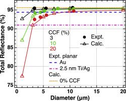
—Patterned-dielectric back contact structures in optoelectronic devices are designed to boost the reflectance of light from the device back surface while retaining a low-resistance pathway for electrical conductance. Their reduced light absorption at near- and sub-bandgap photon energies leads to improved luminescence in light-emitting diodes, greater photon recycling, voltage, and efficiency in photovoltaic cells, and greater recuperation of unabsorbed sub-bandgap light in thermophotovoltaic (TPV) systems. However, diffraction from the patterned features can deflect incident light in propagation directions that lead to light trapping and parasitic absorption in the cell. In this article, we use rigorous coupled-wave analysis (RCWA) to study three-dimensional diffractive scattering of electromagnetic waves by periodic metal point-contact gratings on 1.42-eV GaAs TPV cells, to analyze their effect on unwanted sub-bandgap absorption in order to achieve higher TPV system efficiency. Solutions of Maxwell's equations calculated using RCWA are compared to measured sub-bandgap reflectance in experimental GaAs TPV devices with varying metal point-contact diameters and spacing. Modeling and experiments indicate decreased total reflectance due to these diffractive effects for a small point contact diameter of 1 μm, and this effect is much stronger at higher contact coverage fractions.
Abstract Image

用于砷化镓热光电器件的图案化电介质背触点设计
-光电设备中的图案化介质背接触结构旨在提高设备背表面的光反射率,同时保留低电阻的导电通道。这种结构可减少近带隙和亚带隙光子能量的光吸收,从而改善发光二极管的发光性能,提高光伏电池的光子回收率、电压和效率,并提高热光电(TPV)系统中未被吸收的亚带隙光的回收率。然而,图案化特征的衍射会使入射光在传播方向上发生偏转,从而导致电池中的光捕获和寄生吸收。在本文中,我们采用严格耦合波分析法(RCWA)研究了1.42eV砷化镓冠捷电池上的周期性金属点接触光栅对电磁波的三维衍射散射,分析其对不必要的亚带隙吸收的影响,以实现更高的冠捷系统效率。使用 RCWA 计算出的麦克斯韦方程的解与不同金属点接触直径和间距的实验性砷化镓热塑性硫化器件中测得的亚带隙反射率进行了比较。建模和实验结果表明,在点接触直径为 1 μm 的小范围内,由于这些衍射效应,总反射率会降低,而在接触覆盖率较高时,这种效应会更强。
本文章由计算机程序翻译,如有差异,请以英文原文为准。
求助全文
约1分钟内获得全文 求助全文
来源期刊
Solar Energy Materials and Solar Cells
Solar Energy Materials and Solar Cells 工程技术-材料科学:综合
CiteScore
12.60
自引率
11.60%
发文量
513
审稿时长
47 days
期刊介绍: Solar Energy Materials & Solar Cells is intended as a vehicle for the dissemination of research results on materials science and technology related to photovoltaic, photothermal and photoelectrochemical solar energy conversion. Materials science is taken in the broadest possible sense and encompasses physics, chemistry, optics, materials fabrication and analysis for all types of materials.
×
引用
GB/T 7714-2015
复制
MLA
复制
APA
复制
导出至
BibTeX EndNote RefMan NoteFirst NoteExpress
×
提示
您的信息不完整,为了账户安全,请先补充。
现在去补充
×
提示
您因"违规操作"
具体请查看互助需知
我知道了
×
提示
确定
请完成安全验证×
copy
已复制链接
快去分享给好友吧!
我知道了
右上角分享
点击右上角分享
0
联系我们:info@booksci.cn Book学术提供免费学术资源搜索服务,方便国内外学者检索中英文文献。致力于提供最便捷和优质的服务体验。 Copyright © 2023 布克学术 All rights reserved.
京ICP备2023020795号-1
ghs 京公网安备 11010802042870号
Book学术文献互助
Book学术文献互助群
群 号:481959085
Book学术官方微信