Strain modified nano-scale Ge/Ge0.98Sn0.02 exotic pin photo-sensor array for IR sensing: theoretical reliability and experimental feasibility studies

IF 3.3 3区 工程技术 Q2 ENGINEERING, ELECTRICAL & ELECTRONIC
Bias Bhadra, Suchismita Chinara, Abhijit Kundu
{"title":"Strain modified nano-scale Ge/Ge0.98Sn0.02 exotic pin photo-sensor array for IR sensing: theoretical reliability and experimental feasibility studies","authors":"Bias Bhadra,&nbsp;Suchismita Chinara,&nbsp;Abhijit Kundu","doi":"10.1007/s11082-024-07110-2","DOIUrl":null,"url":null,"abstract":"<div><p>In this paper, the superiority of Ge/Ge<sub>0.98</sub>Sn<sub>0.02</sub>asymmetrical supper lattice structure based vertically doped nano-scale pin photo-sensor under operating wavelength of 1200 nm to 2200 nm is reported. The authors have developed non-linear <b>S</b>train <b>M</b>odified <b>Q</b>uantum-<b>C</b>orrected <b>D</b>rift–<b>D</b>iffusion (<b>SMQCDD</b>) model for analyzing the electrical and optical characteristics of the photo-sensor. The inclusion of a small amount of Sn (2%) into the pure Ge material creates in-plane bi-axial strain in the intrinsic region (i-region) of the device. This results in increases in the value of the out-plane mobility of the charge particles. As a result, the overall performance of the photo-sensor enhances significantly. The authors have used in-plane induced bi-axial strain to accelerate the out-plane mobility of the charge particles by incorporation of the exotic asymmetrical supper lattice structure in the i-region of the photo-sensor. The validation of the non-linear SMQCDD model is performed through comparison of the simulated data obtained from SMQCDD model with the experimental results under a-like thermal/structural/electrical conditions. Additionally, the authors have designed 3X2 array of photo-sensors and studied the photo-electrical characteristics at the said operating wavelength. The proposed device offers better performance in terms of quantum efficiency (0.619: single-type photo-sensor; 0.708: array-type photo) and photo-responsivity (0.056 A/W: single-type photo-sensor; 0.808 A/W:for array-type photo-sensor)at 1600 nm wavelength compared to its conventional flat Si counterpart. The developed exotic pin photo-sensor can be used as a sensing device for applications in optical communication and bio-medical systems. As far as the authors are aware, this is the first report on nano-scale Ge/Ge<sub>0.98</sub>Sn<sub>0.02</sub>exotic pin photo-sensor.</p></div>","PeriodicalId":720,"journal":{"name":"Optical and Quantum Electronics","volume":"56 12","pages":""},"PeriodicalIF":3.3000,"publicationDate":"2024-11-21","publicationTypes":"Journal Article","fieldsOfStudy":null,"isOpenAccess":false,"openAccessPdf":"","citationCount":"0","resultStr":null,"platform":"Semanticscholar","paperid":null,"PeriodicalName":"Optical and Quantum Electronics","FirstCategoryId":"5","ListUrlMain":"https://link.springer.com/article/10.1007/s11082-024-07110-2","RegionNum":3,"RegionCategory":"工程技术","ArticlePicture":[],"TitleCN":null,"AbstractTextCN":null,"PMCID":null,"EPubDate":"","PubModel":"","JCR":"Q2","JCRName":"ENGINEERING, ELECTRICAL & ELECTRONIC","Score":null,"Total":0}
引用次数: 0

Abstract

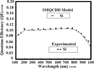
In this paper, the superiority of Ge/Ge0.98Sn0.02asymmetrical supper lattice structure based vertically doped nano-scale pin photo-sensor under operating wavelength of 1200 nm to 2200 nm is reported. The authors have developed non-linear Strain Modified Quantum-Corrected Drift–Diffusion (SMQCDD) model for analyzing the electrical and optical characteristics of the photo-sensor. The inclusion of a small amount of Sn (2%) into the pure Ge material creates in-plane bi-axial strain in the intrinsic region (i-region) of the device. This results in increases in the value of the out-plane mobility of the charge particles. As a result, the overall performance of the photo-sensor enhances significantly. The authors have used in-plane induced bi-axial strain to accelerate the out-plane mobility of the charge particles by incorporation of the exotic asymmetrical supper lattice structure in the i-region of the photo-sensor. The validation of the non-linear SMQCDD model is performed through comparison of the simulated data obtained from SMQCDD model with the experimental results under a-like thermal/structural/electrical conditions. Additionally, the authors have designed 3X2 array of photo-sensors and studied the photo-electrical characteristics at the said operating wavelength. The proposed device offers better performance in terms of quantum efficiency (0.619: single-type photo-sensor; 0.708: array-type photo) and photo-responsivity (0.056 A/W: single-type photo-sensor; 0.808 A/W:for array-type photo-sensor)at 1600 nm wavelength compared to its conventional flat Si counterpart. The developed exotic pin photo-sensor can be used as a sensing device for applications in optical communication and bio-medical systems. As far as the authors are aware, this is the first report on nano-scale Ge/Ge0.98Sn0.02exotic pin photo-sensor.
Abstract Image

用于红外传感的应变修饰纳米级 Ge/Ge0.98Sn0.02 异形引脚光传感器阵列:理论可靠性和实验可行性研究
本文报告了基于垂直掺杂纳米级针式光传感器的 Ge/Ge0.98Sn0.02 不对称 supper 晶格结构在 1200 nm 至 2200 nm 工作波长下的优越性。作者开发了非线性应变修正量子校正漂移扩散(SMQCDD)模型,用于分析光传感器的电气和光学特性。在纯 Ge 材料中加入少量锡(2%)会在器件的本征区(i 区)产生面内双轴应变。这导致电荷粒子面外迁移率值的增加。因此,光传感器的整体性能显著提高。作者在光传感器的 i 区加入了奇特的非对称支撑晶格结构,利用面内诱导双轴应变来加速电荷粒子的面外迁移率。通过将 SMQCDD 模型获得的模拟数据与类似热/结构/电气条件下的实验结果进行比较,验证了非线性 SMQCDD 模型。此外,作者还设计了 3X2 阵列光传感器,并研究了上述工作波长下的光电特性。与传统的平面硅器件相比,所提出的器件在 1600 nm 波长下具有更好的量子效率(0.619:单一型光敏传感器;0.708:阵列型光敏传感器)和光响应率(0.056 A/W:单一型光敏传感器;0.808 A/W:阵列型光敏传感器)。所开发的奇异针形光敏传感器可用作光通信和生物医学系统中的传感设备。据作者所知,这是有关纳米级 Ge/Ge0.98Sn0.02 异种针形光敏传感器的首次报道。
本文章由计算机程序翻译,如有差异,请以英文原文为准。
求助全文
约1分钟内获得全文 求助全文
来源期刊
Optical and Quantum Electronics
Optical and Quantum Electronics 工程技术-工程:电子与电气
CiteScore
4.60
自引率
20.00%
发文量
810
审稿时长
3.8 months
期刊介绍: Optical and Quantum Electronics provides an international forum for the publication of original research papers, tutorial reviews and letters in such fields as optical physics, optical engineering and optoelectronics. Special issues are published on topics of current interest. Optical and Quantum Electronics is published monthly. It is concerned with the technology and physics of optical systems, components and devices, i.e., with topics such as: optical fibres; semiconductor lasers and LEDs; light detection and imaging devices; nanophotonics; photonic integration and optoelectronic integrated circuits; silicon photonics; displays; optical communications from devices to systems; materials for photonics (e.g. semiconductors, glasses, graphene); the physics and simulation of optical devices and systems; nanotechnologies in photonics (including engineered nano-structures such as photonic crystals, sub-wavelength photonic structures, metamaterials, and plasmonics); advanced quantum and optoelectronic applications (e.g. quantum computing, memory and communications, quantum sensing and quantum dots); photonic sensors and bio-sensors; Terahertz phenomena; non-linear optics and ultrafast phenomena; green photonics.
×
引用
GB/T 7714-2015
复制
MLA
复制
APA
复制
导出至
BibTeX EndNote RefMan NoteFirst NoteExpress
×
提示
您的信息不完整,为了账户安全,请先补充。
现在去补充
×
提示
您因"违规操作"
具体请查看互助需知
我知道了
×
提示
确定
请完成安全验证×
copy
已复制链接
快去分享给好友吧!
我知道了
右上角分享
点击右上角分享
0
联系我们:info@booksci.cn Book学术提供免费学术资源搜索服务,方便国内外学者检索中英文文献。致力于提供最便捷和优质的服务体验。 Copyright © 2023 布克学术 All rights reserved.
京ICP备2023020795号-1
ghs 京公网安备 11010802042870号
Book学术文献互助
Book学术文献互助群
群 号:481959085
Book学术官方微信