Double Etch Method for the Fabrication of Nanophotonic Devices from van der Waals Materials

IF 6.5 1区 物理与天体物理 Q1 MATERIALS SCIENCE, MULTIDISCIPLINARY
Otto Cranwell Schaeper, Lesley Spencer, Dominic Scognamiglio, Waleed El-Sayed, Benjamin Whitefield, Jake Horder, Nathan Coste, Paul Barclay, Milos Toth, Anastasiia Zalogina, Igor Aharonovich
{"title":"Double Etch Method for the Fabrication of Nanophotonic Devices from van der Waals Materials","authors":"Otto Cranwell Schaeper, Lesley Spencer, Dominic Scognamiglio, Waleed El-Sayed, Benjamin Whitefield, Jake Horder, Nathan Coste, Paul Barclay, Milos Toth, Anastasiia Zalogina, Igor Aharonovich","doi":"10.1021/acsphotonics.4c02115","DOIUrl":null,"url":null,"abstract":"The integration of van der Waals (vdW) materials into photonic devices has laid out a foundation for many new quantum and optoelectronic applications. Despite tremendous progress in the nanofabrication of photonic building blocks from vdW crystals, there are still limitations, specifically with large-area devices and masking. Here, we focus on hexagonal boron nitride (hBN) as a vdW material and present a double etch method that overcomes problems associated with methods that employ metallic films and resist-based films for masking. Efficacy of the developed protocol is demonstrated by designing and fabricating a set of functional photonic components─including waveguides, ring resonators, and photonic crystal cavities. The functionality of the fabricated structures is demonstrated through optical characterization over several key spectral ranges. These include the near-infrared and blue ranges, where the hBN boron vacancy (V<sub>B</sub><sup>–</sup>) spin defects and the coherent B center quantum emitters emit, respectively. The double etch method enables fabrication of high-quality factor optical cavities and constitutes a promising pathway toward on-chip integration of vdW materials.","PeriodicalId":23,"journal":{"name":"ACS Photonics","volume":"14 1","pages":""},"PeriodicalIF":6.5000,"publicationDate":"2024-11-20","publicationTypes":"Journal Article","fieldsOfStudy":null,"isOpenAccess":false,"openAccessPdf":"","citationCount":"0","resultStr":null,"platform":"Semanticscholar","paperid":null,"PeriodicalName":"ACS Photonics","FirstCategoryId":"101","ListUrlMain":"https://doi.org/10.1021/acsphotonics.4c02115","RegionNum":1,"RegionCategory":"物理与天体物理","ArticlePicture":[],"TitleCN":null,"AbstractTextCN":null,"PMCID":null,"EPubDate":"","PubModel":"","JCR":"Q1","JCRName":"MATERIALS SCIENCE, MULTIDISCIPLINARY","Score":null,"Total":0}
引用次数: 0

Abstract

The integration of van der Waals (vdW) materials into photonic devices has laid out a foundation for many new quantum and optoelectronic applications. Despite tremendous progress in the nanofabrication of photonic building blocks from vdW crystals, there are still limitations, specifically with large-area devices and masking. Here, we focus on hexagonal boron nitride (hBN) as a vdW material and present a double etch method that overcomes problems associated with methods that employ metallic films and resist-based films for masking. Efficacy of the developed protocol is demonstrated by designing and fabricating a set of functional photonic components─including waveguides, ring resonators, and photonic crystal cavities. The functionality of the fabricated structures is demonstrated through optical characterization over several key spectral ranges. These include the near-infrared and blue ranges, where the hBN boron vacancy (VB) spin defects and the coherent B center quantum emitters emit, respectively. The double etch method enables fabrication of high-quality factor optical cavities and constitutes a promising pathway toward on-chip integration of vdW materials.
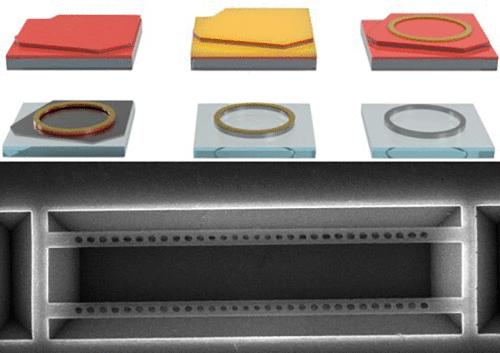
Abstract Image

用范德华材料制造纳米光子器件的双蚀刻法
将范德华(vdW)材料集成到光子设备中为许多新的量子和光电应用奠定了基础。尽管在利用范德华晶体纳米制造光子构件方面取得了巨大进展,但仍然存在一些局限性,特别是在大面积器件和掩膜方面。在此,我们将重点放在作为 vdW 材料的六方氮化硼(hBN)上,并介绍了一种双重蚀刻方法,该方法克服了采用金属薄膜和抗蚀剂薄膜进行掩膜的相关问题。通过设计和制造一组功能性光子元件(包括波导、环形谐振器和光子晶体腔),证明了所开发方案的有效性。通过对几个关键光谱范围进行光学鉴定,证明了所制造结构的功能性。这些光谱范围包括近红外和蓝光,分别是 hBN 硼空位(VB-)自旋缺陷和相干 B 中心量子发射器发射的光谱范围。双蚀刻方法能够制造出高质量的因子光腔,是实现 vdW 材料片上集成的一条大有可为的途径。
本文章由计算机程序翻译,如有差异,请以英文原文为准。
求助全文
约1分钟内获得全文 求助全文
来源期刊
ACS Photonics
ACS Photonics NANOSCIENCE & NANOTECHNOLOGY-MATERIALS SCIENCE, MULTIDISCIPLINARY
CiteScore
11.90
自引率
5.70%
发文量
438
审稿时长
2.3 months
期刊介绍: Published as soon as accepted and summarized in monthly issues, ACS Photonics will publish Research Articles, Letters, Perspectives, and Reviews, to encompass the full scope of published research in this field.
×
引用
GB/T 7714-2015
复制
MLA
复制
APA
复制
导出至
BibTeX EndNote RefMan NoteFirst NoteExpress
×
提示
您的信息不完整,为了账户安全,请先补充。
现在去补充
×
提示
您因"违规操作"
具体请查看互助需知
我知道了
×
提示
确定
请完成安全验证×
copy
已复制链接
快去分享给好友吧!
我知道了
右上角分享
点击右上角分享
0
联系我们:info@booksci.cn Book学术提供免费学术资源搜索服务,方便国内外学者检索中英文文献。致力于提供最便捷和优质的服务体验。 Copyright © 2023 布克学术 All rights reserved.
京ICP备2023020795号-1
ghs 京公网安备 11010802042870号
Book学术文献互助
Book学术文献互助群
群 号:481959085
Book学术官方微信