Ultracompact Polarization-Insensitive 1 × N Silicon-Based Optical Wavelength-Selective Switch by Leveraging I/O Waveguide Spacing Difference

IF 6.5 1区 物理与天体物理 Q1 MATERIALS SCIENCE, MULTIDISCIPLINARY
Zhuping Fan, Xiongshuo Yan, Zhenyu Li, Xiao Ma, Tingting Lang, Dihai Dai, Xuyang Wang, Jun Zou
{"title":"Ultracompact Polarization-Insensitive 1 × N Silicon-Based Optical Wavelength-Selective Switch by Leveraging I/O Waveguide Spacing Difference","authors":"Zhuping Fan, Xiongshuo Yan, Zhenyu Li, Xiao Ma, Tingting Lang, Dihai Dai, Xuyang Wang, Jun Zou","doi":"10.1021/acsphotonics.4c01606","DOIUrl":null,"url":null,"abstract":"Wavelength-selective switches (WSS) have large potential applications in future high-capacity, low-latency, flexible, and energy-efficient data center optical networks. Here, a novel ultracompact 1 × <i>N</i> polarization-insensitive WSS is proposed on the silicon-on-insulator (SOI) platform. The WSS comprises one input port with a polarizing beam splitter and rotator (PBSR), two identical (<i>M</i> × <i>N</i> + 1) × (<i>M</i> + <i>N</i>) arrayed waveguide gratings (AWGs) cascaded with <i>M</i> 1 × <i>N</i> thermo-optic (TO) switches, and <i>N</i> output ports with polarization combiners. The AWG works as both a demultiplexer and multiplexer to eliminate the center wavelength mismatch induced by fabrication errors and to achieve an ultracompact footprint. The TO switches placed on loopback arms allow for the routing of each wavelength to any one of the <i>N</i> output ports. A new design of leveraging the I/O waveguide spacing difference between the loopback inputs and demultiplexing outputs of AWG is employed to eliminate waveguide crossings in a conventional WSS layout design. In experiment, a 12-channel 400 GHz spacing 1 × 2 WSS with a footprint of 1.67 × 1.7 mm<sup>2</sup> is demonstrated. The minimal on-chip loss of 6.8 dB, best extinction ratio of 25 dB, and switching speed of 42 μs are achieved. The measured polarization-dependent loss is &lt;0.5 dB and polarization-dependent wavelength shift is &lt;0.08 nm.","PeriodicalId":23,"journal":{"name":"ACS Photonics","volume":"106 1","pages":""},"PeriodicalIF":6.5000,"publicationDate":"2024-11-19","publicationTypes":"Journal Article","fieldsOfStudy":null,"isOpenAccess":false,"openAccessPdf":"","citationCount":"0","resultStr":null,"platform":"Semanticscholar","paperid":null,"PeriodicalName":"ACS Photonics","FirstCategoryId":"101","ListUrlMain":"https://doi.org/10.1021/acsphotonics.4c01606","RegionNum":1,"RegionCategory":"物理与天体物理","ArticlePicture":[],"TitleCN":null,"AbstractTextCN":null,"PMCID":null,"EPubDate":"","PubModel":"","JCR":"Q1","JCRName":"MATERIALS SCIENCE, MULTIDISCIPLINARY","Score":null,"Total":0}
引用次数: 0

Abstract

Wavelength-selective switches (WSS) have large potential applications in future high-capacity, low-latency, flexible, and energy-efficient data center optical networks. Here, a novel ultracompact 1 × N polarization-insensitive WSS is proposed on the silicon-on-insulator (SOI) platform. The WSS comprises one input port with a polarizing beam splitter and rotator (PBSR), two identical (M × N + 1) × (M + N) arrayed waveguide gratings (AWGs) cascaded with M 1 × N thermo-optic (TO) switches, and N output ports with polarization combiners. The AWG works as both a demultiplexer and multiplexer to eliminate the center wavelength mismatch induced by fabrication errors and to achieve an ultracompact footprint. The TO switches placed on loopback arms allow for the routing of each wavelength to any one of the N output ports. A new design of leveraging the I/O waveguide spacing difference between the loopback inputs and demultiplexing outputs of AWG is employed to eliminate waveguide crossings in a conventional WSS layout design. In experiment, a 12-channel 400 GHz spacing 1 × 2 WSS with a footprint of 1.67 × 1.7 mm2 is demonstrated. The minimal on-chip loss of 6.8 dB, best extinction ratio of 25 dB, and switching speed of 42 μs are achieved. The measured polarization-dependent loss is <0.5 dB and polarization-dependent wavelength shift is <0.08 nm.
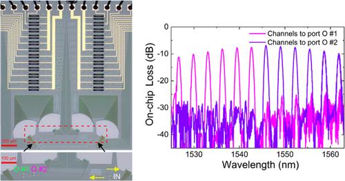
Abstract Image

利用 I/O 波导间距差实现超小型偏振不敏感 1 × N 硅基光波长选择开关
波长选择开关(WSS)在未来大容量、低延迟、灵活和高能效的数据中心光网络中具有巨大的应用潜力。本文在硅绝缘体(SOI)平台上提出了一种新型超小型 1 × N 偏振不敏感 WSS。该 WSS 包括一个带偏振分束器和旋转器 (PBSR) 的输入端口、两个与 M 1 × N 热光学 (TO) 开关级联的相同 (M × N + 1) × (M + N) 阵列波导光栅 (AWG) 以及 N 个带偏振组合器的输出端口。阵列波导光栅既是解复用器,又是多路复用器,可消除由制造误差引起的中心波长失配,并实现超小型占地面积。环回臂上的 TO 开关可将每个波长路由到 N 个输出端口中的任意一个。利用 AWG 回环输入端和解复用输出端之间的 I/O 波导间距差的新设计,消除了传统 WSS 布局设计中的波导交叉。在实验中,演示了一个 12 通道 400 GHz 间距的 1 × 2 WSS,占地面积为 1.67 × 1.7 mm2。芯片上的最小损耗为 6.8 dB,最佳消光比为 25 dB,开关速度为 42 μs。测得的偏振相关损耗为 0.5 dB,偏振相关波长偏移为 0.08 nm。
本文章由计算机程序翻译,如有差异,请以英文原文为准。
求助全文
约1分钟内获得全文 求助全文
来源期刊
ACS Photonics
ACS Photonics NANOSCIENCE & NANOTECHNOLOGY-MATERIALS SCIENCE, MULTIDISCIPLINARY
CiteScore
11.90
自引率
5.70%
发文量
438
审稿时长
2.3 months
期刊介绍: Published as soon as accepted and summarized in monthly issues, ACS Photonics will publish Research Articles, Letters, Perspectives, and Reviews, to encompass the full scope of published research in this field.
×
引用
GB/T 7714-2015
复制
MLA
复制
APA
复制
导出至
BibTeX EndNote RefMan NoteFirst NoteExpress
×
提示
您的信息不完整,为了账户安全,请先补充。
现在去补充
×
提示
您因"违规操作"
具体请查看互助需知
我知道了
×
提示
确定
请完成安全验证×
copy
已复制链接
快去分享给好友吧!
我知道了
右上角分享
点击右上角分享
0
联系我们:info@booksci.cn Book学术提供免费学术资源搜索服务,方便国内外学者检索中英文文献。致力于提供最便捷和优质的服务体验。 Copyright © 2023 布克学术 All rights reserved.
京ICP备2023020795号-1
ghs 京公网安备 11010802042870号
Book学术文献互助
Book学术文献互助群
群 号:481959085
Book学术官方微信