In-situ full-wafer metrology via coupled white light and monochromatic stroboscopic illumination
IF 3.5
2区 工程技术
Q2 OPTICS
引用次数: 0
Abstract
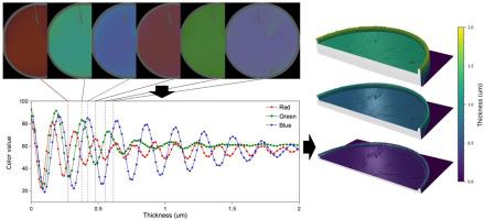
This work presents a novel optical setup to provide scalable in-situ metrology during spin coating. Stroboscopic white light imaging provides high resolution color videos of the process, at a temporal resolution matching the spin speed, where thin film interference colors are observed. Monochromatic specular reflection intensity data from the center of rotation provides a thickness profile at this point. By developing a color to thickness relationship in-situ with the combination of these techniques and leveraging the large-area data provided by color imaging, the thickness at any point on the wafer is reconstructed via a mapping procedure with minimal a-priori information. Experiments are carried out on full 3″ diameter wafers spun with pure xylene or pure butyl acetate, and the thickness profile at all points on the wafer can be determined. Differences in the topology of these solvents whilst drying are linked back to the solvent properties. The color to thickness mapping procedure is shown to have less than 5 % error in determined thickness values between 2μm and 100nm. The possible length scale resolved by the imaging is fully discussed as a function of radius, spin speed, strobe pulse duration and hardware used. The studies in this work achieved a minimum lateral resolution of 315μm when observing a full wafer, which is sufficiently detailed to properly reconstruct thickness variations caused by common spin-coating defects such as comets. The large area and scalable nature of this metrology technique lends itself to applications in semiconductor manufacturing where substrates of 300 mm are standard.

通过耦合白光和单色频闪照明进行原位全晶片测量
这项工作展示了一种新型光学装置,可在旋转镀膜过程中提供可扩展的原位计量。频闪白光成像技术可提供高分辨率的过程彩色视频,其时间分辨率与旋转速度相匹配,在此可观察到薄膜干涉色。来自旋转中心的单色镜面反射强度数据可提供该点的厚度轮廓。通过结合这些技术和利用彩色成像提供的大面积数据,在原位建立起颜色与厚度的关系,从而以最少的先验信息通过映射程序重建晶片上任何一点的厚度。在使用纯二甲苯或纯醋酸丁酯纺丝的直径为 3 英寸的完整晶片上进行实验,可以确定晶片上所有点的厚度轮廓。这些溶剂在干燥过程中的拓扑结构差异与溶剂特性有关。从颜色到厚度的映射程序显示,在 2 微米到 100 纳米之间,确定的厚度值误差小于 5%。成像分辨的可能长度范围作为半径、旋转速度、频闪脉冲持续时间和所用硬件的函数进行了充分讨论。这项工作中的研究在观测整个晶片时实现了最小 315 微米的横向分辨率,其细节足以正确重建由常见旋涂缺陷(如彗星)引起的厚度变化。这种计量技术的大面积和可扩展性使其适合应用于半导体制造领域,在这些领域中,300 毫米的基片是标准基片。
本文章由计算机程序翻译,如有差异,请以英文原文为准。
求助全文
约1分钟内获得全文
求助全文
来源期刊

Optics and Lasers in Engineering
工程技术-光学
CiteScore
8.90
自引率
8.70%
发文量
384
审稿时长
42 days
期刊介绍:
Optics and Lasers in Engineering aims at providing an international forum for the interchange of information on the development of optical techniques and laser technology in engineering. Emphasis is placed on contributions targeted at the practical use of methods and devices, the development and enhancement of solutions and new theoretical concepts for experimental methods.
Optics and Lasers in Engineering reflects the main areas in which optical methods are being used and developed for an engineering environment. Manuscripts should offer clear evidence of novelty and significance. Papers focusing on parameter optimization or computational issues are not suitable. Similarly, papers focussed on an application rather than the optical method fall outside the journal''s scope. The scope of the journal is defined to include the following:
-Optical Metrology-
Optical Methods for 3D visualization and virtual engineering-
Optical Techniques for Microsystems-
Imaging, Microscopy and Adaptive Optics-
Computational Imaging-
Laser methods in manufacturing-
Integrated optical and photonic sensors-
Optics and Photonics in Life Science-
Hyperspectral and spectroscopic methods-
Infrared and Terahertz techniques
 求助内容:
求助内容: 应助结果提醒方式:


