Achieving 11.23 % efficiency in CZTSSe solar cells via defect control and interface contact optimization
IF 6
2区 工程技术
Q2 ENERGY & FUELS
引用次数: 0
Abstract
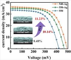
The high open-circuit voltage deficit (VOC, def) caused by structural imperfections in the absorber layer and charge loss during carrier transport is a critical barrier affecting the performance of Cu2ZnSn(S,Se)4 (CZTSSe) devices. In this work, Ag was added to the DMF-based Cu+-Sn4+ system, which significantly improved the crystal morphology and electrical properties of the absorber layer. Additionally, optimizing the selenization process not only reduced surface roughness and eliminated voids at the bottom of the absorber layer but also resulted in the formation of a MoSe2 back interface layer with a more suitable thickness. These measures collectively enhanced the overall quality of the absorber layer, reducing the formation of deep-level defect clusters and effectively boosting carrier transport efficiency. Consequently, the concentration of bulk and interfacial defects decreased, and the impact of potential barriers on carrier movement was minimized. With these comprehensive improvements, the power conversion efficiency of CZTSSe solar cells increased from 8.48 % to 11.23 %. Our research demonstrates that optimizing the structure of the absorber layer can effectively enhance the performance of CZTSSe solar cells, providing valuable insights for the fabrication of high-efficiency devices in the future.

通过缺陷控制和界面接触优化实现 11.23 % 的 CZTSSe 太阳能电池效率
吸收层结构缺陷和载流子传输过程中的电荷损耗导致的高开路电压不足(VOC,def)是影响 Cu2ZnSn(S,Se)4 (CZTSSe) 器件性能的关键障碍。在这项工作中,Ag 被添加到基于 DMF 的 Cu+-Sn4+ 体系中,从而显著改善了吸收层的晶体形态和电性能。此外,优化硒化工艺不仅降低了表面粗糙度,消除了吸收层底部的空隙,还形成了厚度更合适的 MoSe2 背界面层。这些措施共同提高了吸收层的整体质量,减少了深层缺陷簇的形成,有效提高了载流子传输效率。因此,块状缺陷和界面缺陷的浓度降低了,势垒对载流子运动的影响也降到了最低。通过这些综合改进,CZTSSe 太阳能电池的功率转换效率从 8.48% 提高到 11.23%。我们的研究表明,优化吸收层结构可有效提高 CZTSSe 太阳能电池的性能,为未来制造高效器件提供了宝贵的启示。
本文章由计算机程序翻译,如有差异,请以英文原文为准。
求助全文
约1分钟内获得全文
求助全文
来源期刊

Solar Energy
工程技术-能源与燃料
CiteScore
13.90
自引率
9.00%
发文量
0
审稿时长
47 days
期刊介绍:
Solar Energy welcomes manuscripts presenting information not previously published in journals on any aspect of solar energy research, development, application, measurement or policy. The term "solar energy" in this context includes the indirect uses such as wind energy and biomass
 求助内容:
求助内容: 应助结果提醒方式:


