Growth of vertically aligned carbon nanotube bundles by a cost-effective non-lithographic technique for high-performance field emission electron source

IF 3.9 3区 材料科学 Q2 MATERIALS SCIENCE, MULTIDISCIPLINARY
Gulshan Kumar , D.C. Agarwal , Pankaj Srivastava , Santanu Ghosh
{"title":"Growth of vertically aligned carbon nanotube bundles by a cost-effective non-lithographic technique for high-performance field emission electron source","authors":"Gulshan Kumar ,&nbsp;D.C. Agarwal ,&nbsp;Pankaj Srivastava ,&nbsp;Santanu Ghosh","doi":"10.1016/j.mseb.2024.117798","DOIUrl":null,"url":null,"abstract":"<div><div>In the present study, a non-lithographic method is utilized to create patterns of vertically aligned carbon nanotubes (VACNTs). A 20-nm-thick Au layer and a 50-nm-thick Al layer were deposited onto the silicon substrate by thermal evaporation using a steel mesh to create patterns, followed by CNT growth at 900 °C using thermal chemical vapour deposition (TCVD). The effect on the growth of VACNTs on various patterned substrates is studied using a field emission scanning electron microscope (FESEM) and Raman spectroscopy. The field emission characteristics of VACNT bundle patterns produced on patterned surfaces were examined. At 3 V/μm, the current density of CNT film grown on non-patterned substrate is 3.2 mA/cm<sup>2</sup>, which rises to 16.1 mA/cm<sup>2</sup> for the circular pillar of VACNT bundles. Greater spacing between VACNT bundles in the circular pattern reduces electric field screening, resulting in a 500 % increase in current density compared to other samples.</div></div>","PeriodicalId":18233,"journal":{"name":"Materials Science and Engineering B-advanced Functional Solid-state Materials","volume":"311 ","pages":"Article 117798"},"PeriodicalIF":3.9000,"publicationDate":"2024-11-14","publicationTypes":"Journal Article","fieldsOfStudy":null,"isOpenAccess":false,"openAccessPdf":"","citationCount":"0","resultStr":null,"platform":"Semanticscholar","paperid":null,"PeriodicalName":"Materials Science and Engineering B-advanced Functional Solid-state Materials","FirstCategoryId":"88","ListUrlMain":"https://www.sciencedirect.com/science/article/pii/S0921510724006275","RegionNum":3,"RegionCategory":"材料科学","ArticlePicture":[],"TitleCN":null,"AbstractTextCN":null,"PMCID":null,"EPubDate":"","PubModel":"","JCR":"Q2","JCRName":"MATERIALS SCIENCE, MULTIDISCIPLINARY","Score":null,"Total":0}
引用次数: 0

Abstract

In the present study, a non-lithographic method is utilized to create patterns of vertically aligned carbon nanotubes (VACNTs). A 20-nm-thick Au layer and a 50-nm-thick Al layer were deposited onto the silicon substrate by thermal evaporation using a steel mesh to create patterns, followed by CNT growth at 900 °C using thermal chemical vapour deposition (TCVD). The effect on the growth of VACNTs on various patterned substrates is studied using a field emission scanning electron microscope (FESEM) and Raman spectroscopy. The field emission characteristics of VACNT bundle patterns produced on patterned surfaces were examined. At 3 V/μm, the current density of CNT film grown on non-patterned substrate is 3.2 mA/cm2, which rises to 16.1 mA/cm2 for the circular pillar of VACNT bundles. Greater spacing between VACNT bundles in the circular pattern reduces electric field screening, resulting in a 500 % increase in current density compared to other samples.
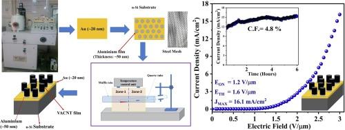
Abstract Image

采用经济高效的非光刻技术生长垂直排列的碳纳米管束,用于高性能场发射电子源
本研究采用非光刻法绘制垂直排列碳纳米管(VACNT)图案。使用钢网通过热蒸发将 20 纳米厚的金层和 50 纳米厚的铝层沉积到硅基底上以创建图案,然后使用热化学气相沉积(TCVD)在 900 °C 下生长碳纳米管。使用场发射扫描电子显微镜(FESEM)和拉曼光谱研究了 VACNT 在不同图案基底上的生长效果。研究了在图案化表面上生成的 VACNT 束图案的场发射特性。在 3 V/μm 的电压下,无图案基底上生长的 CNT 薄膜的电流密度为 3.2 mA/cm2,而 VACNT 束的圆柱形电流密度则上升到 16.1 mA/cm2。圆形图案中 VACNT 束之间的间距增大,减少了电场屏蔽,使电流密度比其他样品提高了 500%。
本文章由计算机程序翻译,如有差异,请以英文原文为准。
求助全文
约1分钟内获得全文 求助全文
来源期刊
CiteScore
5.60
自引率
2.80%
发文量
481
审稿时长
3.5 months
期刊介绍: The journal provides an international medium for the publication of theoretical and experimental studies and reviews related to the electronic, electrochemical, ionic, magnetic, optical, and biosensing properties of solid state materials in bulk, thin film and particulate forms. Papers dealing with synthesis, processing, characterization, structure, physical properties and computational aspects of nano-crystalline, crystalline, amorphous and glassy forms of ceramics, semiconductors, layered insertion compounds, low-dimensional compounds and systems, fast-ion conductors, polymers and dielectrics are viewed as suitable for publication. Articles focused on nano-structured aspects of these advanced solid-state materials will also be considered suitable.
×
引用
GB/T 7714-2015
复制
MLA
复制
APA
复制
导出至
BibTeX EndNote RefMan NoteFirst NoteExpress
×
提示
您的信息不完整,为了账户安全,请先补充。
现在去补充
×
提示
您因"违规操作"
具体请查看互助需知
我知道了
×
提示
确定
请完成安全验证×
copy
已复制链接
快去分享给好友吧!
我知道了
右上角分享
点击右上角分享
0
联系我们:info@booksci.cn Book学术提供免费学术资源搜索服务,方便国内外学者检索中英文文献。致力于提供最便捷和优质的服务体验。 Copyright © 2023 布克学术 All rights reserved.
京ICP备2023020795号-1
ghs 京公网安备 11010802042870号
Book学术文献互助
Book学术文献互助群
群 号:481959085
Book学术官方微信