Formation of 2H and 1T/2H MoSe2 via thermal selenization of electrodeposited Mo thin films and nanowires
IF 6.3
2区 材料科学
Q2 CHEMISTRY, PHYSICAL
引用次数: 0
Abstract
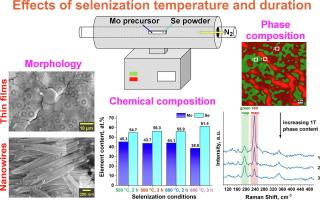
Here, we present how thermal selenization can be used in tandem with electrodeposition to prepare MoSe2-based materials. Mo precursors (thin films or nanowire arrays) were prepared via electrodeposition and thermally selenized at 500/600 °C for 2/3h. Scanning electron microscopy (FE-SEM), X-ray powder diffraction (XRD), energy-dispersive X-ray spectroscopy (EDS), X-ray photoelectron spectroscopy (XPS), and Raman spectroscopy were used to determine the morphology, chemical and phase compositions of materials. The experimental results demonstrated changes in the morphology after selenization, like creation of circular grain domains in Mo films, and partial hollowing and coarsening of Mo nanowires. Selenization of both types of precursors resulted in phase-diverse MoSe2 products: hexagonal (2H) phase for Mo films, and mixture of trigonal and hexagonal (1T/2H) phases in the case of Mo nanowires. EDS measurements revealed that the Se content in Mo-Se films varied from 4.6 to 26.5 at.%, while in Mo-Se nanowires, it ranged from 54.7 to 61.4 at.%, which indicates that thermal selenization was more effective when the precursor was in the form of nanowires. This study suggests the potential to control parameters in the thermal selenization process such as substrate selection, temperature, and duration to develop innovative MoSe2-based electrodes for more efficient energy-related applications.

通过电沉积钼薄膜和纳米线的热硒化形成 2H 和 1T/2H MoSe2
在此,我们介绍了如何将热硒化与电沉积同时用于制备基于 MoSe2 的材料。钼前驱体(薄膜或纳米线阵列)通过电沉积制备,并在 500/600 °C 下热硒化 2/3 小时。使用扫描电子显微镜(FE-SEM)、X 射线粉末衍射(XRD)、能量色散 X 射线光谱(EDS)、X 射线光电子能谱(XPS)和拉曼光谱测定材料的形态、化学成分和相组成。实验结果表明,硒化后的材料形态发生了变化,如 Mo 薄膜中产生了圆形晶域,Mo 纳米线部分空心化和粗化。对这两种前驱体进行硒化后,会产生相态多样的 MoSe2 产物:钼薄膜为六方(2H)相,而钼纳米线则为三方和六方(1T/2H)混合相。EDS 测量显示,钼-硒薄膜中的硒含量从 4.6% 到 26.5% 不等,而钼-硒纳米线中的硒含量则从 54.7% 到 61.4% 不等,这表明当前驱体为纳米线形式时,热硒化更为有效。这项研究表明,通过控制热硒化过程中的参数(如基底选择、温度和持续时间),有可能开发出基于 MoSe2 的创新电极,用于更高效的能源相关应用。
本文章由计算机程序翻译,如有差异,请以英文原文为准。
求助全文
约1分钟内获得全文
求助全文
来源期刊

Applied Surface Science
工程技术-材料科学:膜
CiteScore
12.50
自引率
7.50%
发文量
3393
审稿时长
67 days
期刊介绍:
Applied Surface Science covers topics contributing to a better understanding of surfaces, interfaces, nanostructures and their applications. The journal is concerned with scientific research on the atomic and molecular level of material properties determined with specific surface analytical techniques and/or computational methods, as well as the processing of such structures.
 求助内容:
求助内容: 应助结果提醒方式:


