Soundarya Nagarajan, Ingmar Ratschinski, Stefan Schmult, Steffen Wirth, Dirk König, Thomas Mikolajick, Daniel Hiller, Jens Trommer
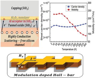
{"title":"Analyzing Carrier Density and Hall Mobility in Impurity-Free Silicon Virtually Doped by External Defect Placement","authors":"Soundarya Nagarajan, Ingmar Ratschinski, Stefan Schmult, Steffen Wirth, Dirk König, Thomas Mikolajick, Daniel Hiller, Jens Trommer","doi":"10.1002/adfm.202415230","DOIUrl":null,"url":null,"abstract":"<p>Impurity doping at the nanoscale for silicon is becoming less efficient with conventional techniques. Here, an alternative virtual doping method is presented for silicon that can achieve an equivalent carrier density while addressing the primary limitations of traditional doping methods. The doping for silicon is carried out by placing aluminum-induced acceptor states externally in a silicon dioxide dielectric shell. This technique can be referred to as direct modulation doping. The resistivity, carrier density, and mobility are investigated by Hall effect measurements to characterize the carrier transport using the new doping method. The results thereof are compared with carrier transport analysis of conventionally doped silicon at room-temperature, demonstrating a 100% increase in carrier mobility at equal carrier density. The sheet density of hole carriers in silicon due to modulation doping remains nearly constant, ≈4.7 × 10<sup>12</sup> cm<sup>−2</sup> over a wide temperature range from 300 down to 2 K, proving that modulation-doped devices do not undergo carrier freeze-out at cryogenic temperatures. In addition, a mobility enhancement is demonstrated with an increase from 89 cm<sup>2</sup> Vs<sup>−1</sup> at 300 K to 227 cm<sup>2</sup> Vs<sup>−1</sup> at 10 K, highlighting the benefits of the new method for creating emerging nanoscale electronic devices or peripheral cryo-electronics to quantum computing.</p>","PeriodicalId":112,"journal":{"name":"Advanced Functional Materials","volume":"35 7","pages":""},"PeriodicalIF":18.5000,"publicationDate":"2024-11-13","publicationTypes":"Journal Article","fieldsOfStudy":null,"isOpenAccess":false,"openAccessPdf":"","citationCount":"0","resultStr":null,"platform":"Semanticscholar","paperid":null,"PeriodicalName":"Advanced Functional Materials","FirstCategoryId":"88","ListUrlMain":"https://onlinelibrary.wiley.com/doi/10.1002/adfm.202415230","RegionNum":1,"RegionCategory":"材料科学","ArticlePicture":[],"TitleCN":null,"AbstractTextCN":null,"PMCID":null,"EPubDate":"","PubModel":"","JCR":"Q1","JCRName":"CHEMISTRY, MULTIDISCIPLINARY","Score":null,"Total":0}
引用次数: 0
Abstract
Impurity doping at the nanoscale for silicon is becoming less efficient with conventional techniques. Here, an alternative virtual doping method is presented for silicon that can achieve an equivalent carrier density while addressing the primary limitations of traditional doping methods. The doping for silicon is carried out by placing aluminum-induced acceptor states externally in a silicon dioxide dielectric shell. This technique can be referred to as direct modulation doping. The resistivity, carrier density, and mobility are investigated by Hall effect measurements to characterize the carrier transport using the new doping method. The results thereof are compared with carrier transport analysis of conventionally doped silicon at room-temperature, demonstrating a 100% increase in carrier mobility at equal carrier density. The sheet density of hole carriers in silicon due to modulation doping remains nearly constant, ≈4.7 × 1012 cm−2 over a wide temperature range from 300 down to 2 K, proving that modulation-doped devices do not undergo carrier freeze-out at cryogenic temperatures. In addition, a mobility enhancement is demonstrated with an increase from 89 cm2 Vs−1 at 300 K to 227 cm2 Vs−1 at 10 K, highlighting the benefits of the new method for creating emerging nanoscale electronic devices or peripheral cryo-electronics to quantum computing.
期刊介绍:
Firmly established as a top-tier materials science journal, Advanced Functional Materials reports breakthrough research in all aspects of materials science, including nanotechnology, chemistry, physics, and biology every week.
Advanced Functional Materials is known for its rapid and fair peer review, quality content, and high impact, making it the first choice of the international materials science community.

 求助内容:
求助内容: 应助结果提醒方式:


