Production of Ultrathin and High-Quality Nanosheet Networks via Layer-by-Layer Assembly at Liquid–Liquid Interfaces
IF 16
1区 材料科学
Q1 CHEMISTRY, MULTIDISCIPLINARY
引用次数: 0
Abstract
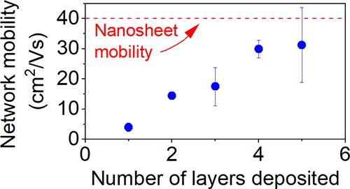
Solution-processable 2D materials are promising candidates for a range of printed electronics applications. Yet maximizing their potential requires solution-phase processing of nanosheets into high-quality networks with carrier mobility (μNet) as close as possible to that of individual nanosheets (μNS). In practice, the presence of internanosheet junctions generally limits electronic conduction, such that the ratio of junction resistance (RJ) to nanosheet resistance (RNS), determines the network mobility via μNS/μNet ≈ RJ/RNS + 1. Hence, achieving RJ/RNS < 1 is a crucial step for implementation of 2D materials in printed electronics applications. In this work, we utilize an advanced liquid-interface deposition process to maximize nanosheet alignment and network uniformity, thus reducing RJ. We demonstrate the approach using graphene and MoS2 as model materials, achieving low RJ/RNS values of 0.5 and 0.2, respectively. The resultant graphene networks show a high conductivity of σNet = 5 × 10⁴ S/m while our semiconducting MoS2 networks demonstrate record mobility of μNet = 30 cm2/(V s), both at extremely low network thickness (tNet < 10 nm). Finally, we show that the deposition process is compatible with nonlayered quasi-2D materials such as silver nanosheets (AgNS), achieving network conductivity close to bulk silver for networks <100 nm-thick.
通过在液-液界面逐层组装生产超薄和高质量纳米片网络
可溶液加工的二维材料是一系列印刷电子应用的理想候选材料。然而,要最大限度地发挥这些材料的潜力,需要将纳米片溶液相加工成高质量的网络,使其载流子迁移率(μNet)尽可能接近单个纳米片的迁移率(μNS)。实际上,纳米片间结的存在通常会限制电子传导,因此结电阻(RJ)与纳米片电阻(RNS)之比通过μNS/μNet ≈ RJ/RNS + 1 决定了网络的迁移率。因此,实现 RJ/RNS < 1 是在印刷电子应用中实现二维材料的关键一步。在这项工作中,我们利用先进的液面沉积工艺,最大限度地提高纳米片对齐度和网络均匀性,从而降低 RJ。我们以石墨烯和 MoS2 为模型材料演示了这种方法,其 RJ/RNS 值分别低至 0.5 和 0.2。由此产生的石墨烯网络显示出 σNet = 5 × 10⁴ S/m 的高电导率,而我们的半导体 MoS2 网络则显示出 μNet = 30 cm2/(V s) 的创纪录迁移率,两者都是在网络厚度极低(tNet < 10 nm)的情况下实现的。最后,我们还展示了该沉积工艺与银纳米片(AgNS)等非层状准二维材料的兼容性,在厚度为 100 nm 的网络中实现了接近于体银的网络导电性。
本文章由计算机程序翻译,如有差异,请以英文原文为准。
求助全文
约1分钟内获得全文
求助全文
来源期刊

ACS Nano
工程技术-材料科学:综合
CiteScore
26.00
自引率
4.10%
发文量
1627
审稿时长
1.7 months
期刊介绍:
ACS Nano, published monthly, serves as an international forum for comprehensive articles on nanoscience and nanotechnology research at the intersections of chemistry, biology, materials science, physics, and engineering. The journal fosters communication among scientists in these communities, facilitating collaboration, new research opportunities, and advancements through discoveries. ACS Nano covers synthesis, assembly, characterization, theory, and simulation of nanostructures, nanobiotechnology, nanofabrication, methods and tools for nanoscience and nanotechnology, and self- and directed-assembly. Alongside original research articles, it offers thorough reviews, perspectives on cutting-edge research, and discussions envisioning the future of nanoscience and nanotechnology.
 求助内容:
求助内容: 应助结果提醒方式:


