Electrochemical-induced morphological formation and optical properties of p-type silicon wafer

IF 1.9 4区 材料科学 Q3 MATERIALS SCIENCE, MULTIDISCIPLINARY
Mohd Norizam Md Daud, Mohamad Firdaus Mohamad Noh, Nurul Affiqah Arzaee, Amin Aadenan, Danial Hakim Badrul Hisham, Muhammad Athir Mohamed Anuar, Mohd Adib Ibrahim, Suhaila Sepeai, Mohd Asri Mat Teridi
{"title":"Electrochemical-induced morphological formation and optical properties of p-type silicon wafer","authors":"Mohd Norizam Md Daud,&nbsp;Mohamad Firdaus Mohamad Noh,&nbsp;Nurul Affiqah Arzaee,&nbsp;Amin Aadenan,&nbsp;Danial Hakim Badrul Hisham,&nbsp;Muhammad Athir Mohamed Anuar,&nbsp;Mohd Adib Ibrahim,&nbsp;Suhaila Sepeai,&nbsp;Mohd Asri Mat Teridi","doi":"10.1007/s12034-024-03349-3","DOIUrl":null,"url":null,"abstract":"<div><p>The enhancement of light absorption and surface area in monocrystalline solar cells is achieved through anisotropic etching, with the aim of improving its conversion efficiency. Nevertheless, the conventional method of anisotropic etching is constrained in its capacity for incrementing surface area. Herein, a promising texturization process in the form of a homogenous and uniform pyramidal structure is proposed with two-step texturing processes: cyclic voltammetry (CV) treatment and the alkali anisotropic etching method on the silicon wafer surface. Prior to and following the alkali texturing process, the silicon surface was modified using the CV treatment. The effect of this approach was investigated under different CV cycles (20, 40, 60 and 80 cycles) in a 0.5 M Na<sub>2</sub>SO<sub>4</sub> aqueous electrolyte with pH ~ 7. Based on the field emission scanning electron microscope (FESEM) micrographs and UV-visible spectrometer (UV-Vis) measurements, the wafer textured with 60 cycles of CV treatment and an alkali anisotropic etching process tremendously improves the surface morphology and decreases the front surface reflection. As a result, the size and height of the pyramid formed were 2.1–2.3 µm and 0.6–1.9 µm, respectively. Moreover, the outlined methodology facilitates a substantial decrease in surface damage and is applicable in the Si texturization process for the manufacturing of solar cells.</p></div>","PeriodicalId":502,"journal":{"name":"Bulletin of Materials Science","volume":"47 4","pages":""},"PeriodicalIF":1.9000,"publicationDate":"2024-11-09","publicationTypes":"Journal Article","fieldsOfStudy":null,"isOpenAccess":false,"openAccessPdf":"","citationCount":"0","resultStr":null,"platform":"Semanticscholar","paperid":null,"PeriodicalName":"Bulletin of Materials Science","FirstCategoryId":"88","ListUrlMain":"https://link.springer.com/article/10.1007/s12034-024-03349-3","RegionNum":4,"RegionCategory":"材料科学","ArticlePicture":[],"TitleCN":null,"AbstractTextCN":null,"PMCID":null,"EPubDate":"","PubModel":"","JCR":"Q3","JCRName":"MATERIALS SCIENCE, MULTIDISCIPLINARY","Score":null,"Total":0}
引用次数: 0

Abstract

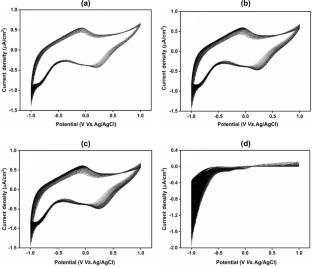
The enhancement of light absorption and surface area in monocrystalline solar cells is achieved through anisotropic etching, with the aim of improving its conversion efficiency. Nevertheless, the conventional method of anisotropic etching is constrained in its capacity for incrementing surface area. Herein, a promising texturization process in the form of a homogenous and uniform pyramidal structure is proposed with two-step texturing processes: cyclic voltammetry (CV) treatment and the alkali anisotropic etching method on the silicon wafer surface. Prior to and following the alkali texturing process, the silicon surface was modified using the CV treatment. The effect of this approach was investigated under different CV cycles (20, 40, 60 and 80 cycles) in a 0.5 M Na2SO4 aqueous electrolyte with pH ~ 7. Based on the field emission scanning electron microscope (FESEM) micrographs and UV-visible spectrometer (UV-Vis) measurements, the wafer textured with 60 cycles of CV treatment and an alkali anisotropic etching process tremendously improves the surface morphology and decreases the front surface reflection. As a result, the size and height of the pyramid formed were 2.1–2.3 µm and 0.6–1.9 µm, respectively. Moreover, the outlined methodology facilitates a substantial decrease in surface damage and is applicable in the Si texturization process for the manufacturing of solar cells.
Abstract Image

电化学诱导的 p 型硅晶片形貌形成和光学特性
通过各向异性蚀刻,可以增强单晶硅太阳能电池的光吸收和表面积,从而提高其转换效率。然而,传统的各向异性蚀刻方法在增加表面积方面受到限制。在此,我们提出了一种很有前景的制绒工艺,即在硅晶片表面采用两步制绒工艺制备均匀一致的金字塔结构:循环伏安法(CV)处理和碱各向异性蚀刻法。在碱制绒工艺之前和之后,使用循环伏安法对硅表面进行了改性。在 pH 值为 7 ~ 7 的 0.5 M Na2SO4 水电解液中,研究了不同 CV 周期(20、40、60 和 80 个周期)下这种方法的效果。根据场发射扫描电子显微镜(FESEM)显微照片和紫外-可见光谱仪(UV-Vis)的测量结果,经过 60 次 CV 处理和碱各向异性蚀刻工艺制备纹理的晶片极大地改善了表面形貌,减少了正面反射。因此,形成的金字塔尺寸和高度分别为 2.1-2.3 µm 和 0.6-1.9 µm。此外,所概述的方法有助于大幅减少表面损伤,适用于制造太阳能电池的硅纹理化工艺。
本文章由计算机程序翻译,如有差异,请以英文原文为准。
求助全文
约1分钟内获得全文 求助全文
来源期刊
Bulletin of Materials Science
Bulletin of Materials Science 工程技术-材料科学:综合
CiteScore
3.40
自引率
5.60%
发文量
209
审稿时长
11.5 months
期刊介绍: The Bulletin of Materials Science is a bi-monthly journal being published by the Indian Academy of Sciences in collaboration with the Materials Research Society of India and the Indian National Science Academy. The journal publishes original research articles, review articles and rapid communications in all areas of materials science. The journal also publishes from time to time important Conference Symposia/ Proceedings which are of interest to materials scientists. It has an International Advisory Editorial Board and an Editorial Committee. The Bulletin accords high importance to the quality of articles published and to keep at a minimum the processing time of papers submitted for publication.
×
引用
GB/T 7714-2015
复制
MLA
复制
APA
复制
导出至
BibTeX EndNote RefMan NoteFirst NoteExpress
×
提示
您的信息不完整,为了账户安全,请先补充。
现在去补充
×
提示
您因"违规操作"
具体请查看互助需知
我知道了
×
提示
确定
请完成安全验证×
copy
已复制链接
快去分享给好友吧!
我知道了
右上角分享
点击右上角分享
0
联系我们:info@booksci.cn Book学术提供免费学术资源搜索服务,方便国内外学者检索中英文文献。致力于提供最便捷和优质的服务体验。 Copyright © 2023 布克学术 All rights reserved.
京ICP备2023020795号-1
ghs 京公网安备 11010802042870号
Book学术文献互助
Book学术文献互助群
群 号:481959085
Book学术官方微信